Populating the Main PCB
Now that your power supply is built and tested, you can proceed with populating the rest of the PCBs. Start by printing the parts list. I like to cross out each component as it's soldered into place. In addition to a soldering iron and a digital multimeter (DMM), you’ll need some lead trimmers and a lead bender or needle nose pliers. This lead bender is Mouser part 5166-801, but a pair a needle nose pliers will work just as well.
Enough! Let’s populate this bastard!
Diodes
PCBs are generally populated by starting with the smaller components that sit close to the PCB and ending with the taller and larger components. The diodes are as good a place as any to start. There are generally a few different types in the FET Compressor. The four 1N4004 diodes are used in the power supply as a bridge rectifier to convert your AC to DC. There are two FDH333 diodes in the gain reduction amp that convert your gain reduction amp signal to a DC voltage for your FET gates, and one 1N914 and 1N4740A diode. Your diode will have its name (FDH333, 1N4004, 1N914..) printed on the diode itself. Look really close!
It's important to note that regardless of the type, diodes are polarized devices. Specifically, they have a positive (anode) and negative (cathode) lead. They must be inserted properly to work. On your diode you will notice one lead is marked with a line. This line indicates the negative or cathode lead. The silkscreen also shows the diode with a line at one side. This indicates how the diode should be inserted. Pretty easy!
Notice how the line on the diode is on the same side as the line on the silkscreen layer in the image above.
Resistors
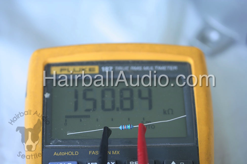
Time to grab a beer, brew a coffee, or put on your favorite record. This one will take a while. Take your time, misplacing a 270Ω for a 270KΩ resistor is not an easy thing to sort out when your build doesn’t work right. Test each resistor with your DMM Ω setting before soldering it in place. You'll rest easy later on.
I know my resistor color band codes, but I’ve checked this 150KΩ resistor anyway. Not only have I double checked my eyes, I’ve confirmed it’s working correctly. Resistors are not polarized. You can insert them in either direction. Take your time (really, please TAKE YOUR TIME), the extra time taken now can save you hours or days of troubleshooting.
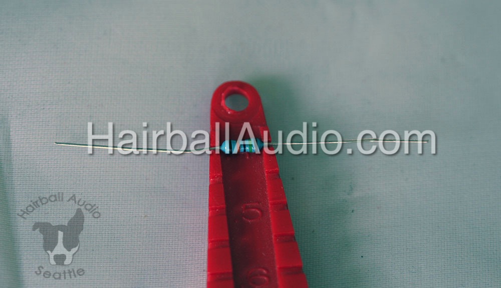
Shown above is a resistor ready for lead bending.
Resistors stuffed in a rev A PCB.
Transistors
We could go a few different directions at this point, but lets move to transistors. These have three leads. The majority of the transistors in the FET Compressor are actually not FETs, but BJTs or Bipolar Junction Transistors. These have a collector, an emitter, and a base. These can vary from component to component so to make it easy for you, the PCB silk-screen matches the package of the transistors. Most are T0-92 packages which look like a “D” from the top and align with the “D” on the silk-screen.
Q1 and Q11 are the FETs of the FET Compressor (The Rev A also has some J309 FETs). Q1 is the compression FET and Q11 controls the meters GR display. These FET leads are a source, drain, and gate. Again they are TO-92 types (D-shaped). These FETs have their transfer curve matched to within 10% to ensure your meter and the actual GR are the same. You’d be surprised how widely transistors can vary out of the same box.
Your compressor also has a TO-39 transistor (2N3053) Q6 which has a tab that should line up with the silk-screen tab.
This transistor also needs to have a heat-sink (supplied) clipped onto it to avoid thermal runoff. You may want to wait until the board is fully stuffed to add the heat-sink. Your heat-sink may look like the one pictured below or appear more disc shaped.
Before we proceed, we need to test our BJTs for hFE. hFE is a measure of current gain and the pair of transistors (Q12 and Q13) in the meter section require hFE to be closely matched. The BJT also need to have a fairly high hFE. I have found the 2N3707 marked on the MNATS PCB to be a little too low so I have substituted them with 2N3708 transistors. These are similar but with a higher hFE. To match two for your meter section, it helps to have a meter that can test for hFE. I have this $30 meter (Velleman DVM890F) which does a nice job.
You can see that it has an hFE dial setting and sockets for PNP and PNP transistors above. Next identify the pinout of the transistor and insert it into the sockets to attain an hFE reading. The 3707/2N3708 are NPN transistors. By looking up the datasheet I’ve been able to determine the leads.
Now insert it on the NPN side matching the leads to their proper socket.
The transistor pictured has an hFE of 426. Measure the hFE of all the 2N3708 devices and select two that are close (10%) to use in Q12 and Q13. For example a good match for this transistor with and hFE of 426 would be a transistor between 384 and 468. I bet you can get a lot closer than that.
Here you can see the TO-92 2N3708 mounted. Note that for the TO-92 types we’ve used the three identical pads in a line.
Trim Pots
Let’s talk trim pots. These trip a lot of people up and it can be a little confusing. Let’s clear up the two major issues. Why are you missing one, and how do you mount them?
Let’s start with the missing trim pot. You'll note you're missing a 2K trim pot. However, you’ll also have an extra 2K panel mount pot. Hmmmmm. Here is the scoop, for the zero adjust pot, you should use the 2K panel mount pot in the control bag. This trimmer is R71 on the silkscreen and having a panel mounted pot allows you to easily set the zero on the meter with a screwdriver through a small hole on the front panel. Leave it empty for now, we'll install the zero adjust pot in the wiring section.
Before we talk about the second issue, how to mount them, lets get them ready to mount. The trim pot is essentially a variable resistor. It has three legs. If it’s a 2K trim pot, there is a 2KΩ resistance between the two outer leads. The middle lead, the wiper, slides back and forth between them and is controlled by the screw. If the wiper is rotated all the way right, there will be near 0Ω resistance between the wiper and the right lead and near 2KΩ between the wiper and the left lead. Rotate it all the way to the other side and they will be opposite.
These pots take 20 turns to move from one side to the other. They also do not have a “stop” so they keep rotating even when they have reached the end. Rotate them enough and they will break. For this reason I think it’s a good idea to set the wiper in the middle to start. Take your DMM and use the Ω setting. Test between the wiper and one of the outer leads. Set the screw so the Ω is 1/2 of the pot value. For a 2K pot this would be 1KΩ.
Now let's mount them on the PCB. The silk-screen displayed is for a different trim pot style than the Bourns trimmers supplied. If you were to insert the Bourns type supplied according to the silk-screen, all the leads would be shorted together. Not a very useful trim pot. Pads are provided for the Bourns types, just don’t follow the screen. Note how they are installed correctly here. Also note the screw position as it relates to the existing screen. Finally note that I have left R71 empty! Remember we’ll use the panel mounted pot here in the next section on wiring.
Rev A (3 trimmers):
Rev D (4 trimmers):
Capacitors
Let's talk capacitors!
Here are the types you'll use in your build. The electrolytic and tantalum capacitors are polarized and must be inserted in the right direction. The film and ceramic capacitors are not polarized. The larger "Orange Drop" capacitors are only found in the rev A build.
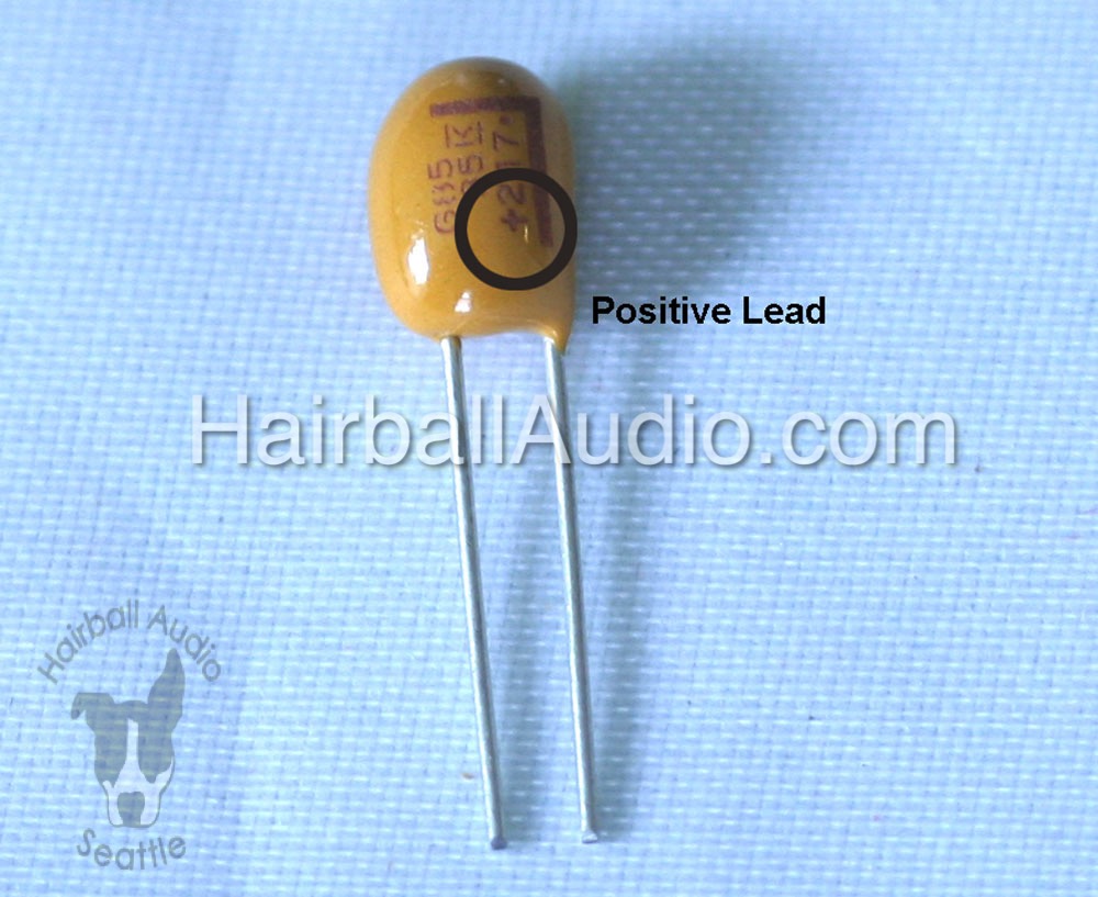
The value of the capacitor will help you determine where it will be placed as will following the BOM. One important note is that the two 6.8uF tantalum capacitors should be used in the gain reduction amp designations C19 and C20. They are polarized and the positive lead is marked with a black line and a +. This lead should be entered into the pad marked “+” on the C19/C20 silk-screen.
Electrolytics are also polarized. Like diodes,it is their negative lead that is marked. The opposite and unmarked lead is the positive and it is placed into the pad on the silk-screen marked with a “+”.
The film and ceramic capacitors are non polarized and can be inserted in either direction. Recently we've changed some of the film capacitors because we thought they sounded closer to the original UREI 1176. Our film caps are now generally grey or cream colored. Identifying the value can be a little tricky. Note that film caps generally range in value from 0.001uF up to 1uF. The grey caps tend to show their value in Nano Farad (nF). To convert nF to uF move the decimal three places to the left.
Example:
33n = 33nF = 0.033uF
4n7 = 4.7nF = 0.0047uF
1n = 1nF = 0.001uF
220n = 220nF = 0.22uF
22n = 22nF = 0.022uF
The cream caps usually just indicate the uF value. So 1 = 1uF and .15 = 0.15uF. Ignore letters like J and K and the numbers after them. They are generally tolerance and date codes.
Some footprints have extra pads for wider capacitors. Note that one set of pads will be all connected and the other will be all connected. Make sure regardless of width your capacitor pads are not inserted on the same set of pads and shorted to one another. You may have some with kinked leads, push hard and snap them into place. It’s pretty straight forward.
Four film capacitors in the rev A build are large "Orange Drop" types. C2/C8 are the smaller 0.15uF capacitors and C7/C10 are the larger 1uF capacitors.
Orange Drop capacitor placement. There are multiple pads for each lead. The group of pads on each side are connected, just place the capacitor where they fit making sure one lead is on one half and the other lead is on the other. Even though C7/C10 show a + for polarity you can ignore it. The Orange Drops are not polarized.
The smaller ceramic caps have three numbers indicating their value in pF. The first two numbers are literal and the third is the number of zeros.
Example:
100 = 10pF
200 = 20pF
201 = 200pF
682 = 6800pF
Wire Headers
Headers are optional. I like using them on the main PCB, but you can choose to solder directly to the pads instead of using headers. Headers have the advantage of easy wire removal if you make a wiring error; however, the connection is not as secure as a direct solder connection and the pad numbers get covered. If you choose to use the headers, insert them with the wire receiving side or slanted side facing out. You can see the pad numbers that are now covered by downloading the MNATS PCB document for your revision.
Revision A 1.2.5
Revison D 2.2
Pictured is the end that accepts the wire and faces out from the PCB.
3 Pin Header and Jumper
Your compressor has a discrete (no microchips) meter section just like the original units. During the calibration of the circuit you’ll need to take R44 out of circuit. This is done using a 3 pin header with a jumper plug. You can see it inserted here next to R44 and it’s in the default R44 in circuit position.
Note that for the Rev A we've soldered two clipped diode leads into TP10 and TP11. This is not necessary, however it'll give you something to clip your DMM leads to when you reach calibration. These points are not used on the rev D.
Below is a fully populated revision A PCB. Note R71 is a wired pot as mentioned earlier. Ignore that for now, we'll add it later.
Here is a fully populated revision D PCB.
Populating the Ratio PCB
The ratio PCB controls both the ratio of compression and the fixed threshold. It is basically two resistor ladders controlled by DPDT switches. The PCB has some documentation on it. In the upper right it shows a PAD guide which you’ll use in the wiring step. It also has the 10 resistors needed to form the resistor ladders. They have no values listed and are simply marked with R1-R10. This is because the actual designated names and values vary from revision to revision. The resistor value is listed for each revision in the table below. The name in brackets is the designation on the schematic and BOM.
| Ratio PCB | Rev A | Rev D |
| R1 | (R58) = 120Ω | (R58) = 150Ω |
| R2 | (R61) = 470Ω | (R61) = 470Ω |
| R3 | (R62) = 470Ω | (R62) = 560Ω |
| R4 | (R63) = 1.5KΩ | (R63) = 1.5KΩ |
| R5 | (R45) = 10MΩ | (R45) = 10MΩ |
| R6 | (R21) = 56KΩ | (R21) = 56KΩ |
| R7 | (R20) = 56KΩ | (R20) = 56KΩ |
| R8 | (R19) = 68KΩ | (R19) = 68KΩ |
| R9 | (R22) = 47KΩ | (R22) = 47KΩ |
| R10 | (R78) = 47KΩ | (R78) = 56KΩ |
The KK series wire headers for the ratio and meter PCB are not included in the kit as they require a special crimping tool and technique. I prefer to wire directly to the solder pads with these PCBs.
Mounting the Input Transformer
The input transformer used in the kit is a reproduction of the original UTC O-12 transformer.
When mounting the transformer you need to make sure it is oriented correctly. The dot on the label identifies pin 1. Insert that pin into the pad marked with a “1”. Here is the complete PCB with optional wire headers.
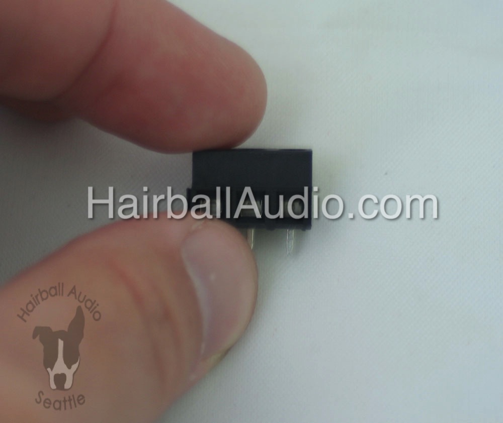
Mounting the tpad is very straight forward and it can only be inserted in one direction.
You’ve made it! You’re now ready for the next step, wiring your FET Compressor.

