Introduction
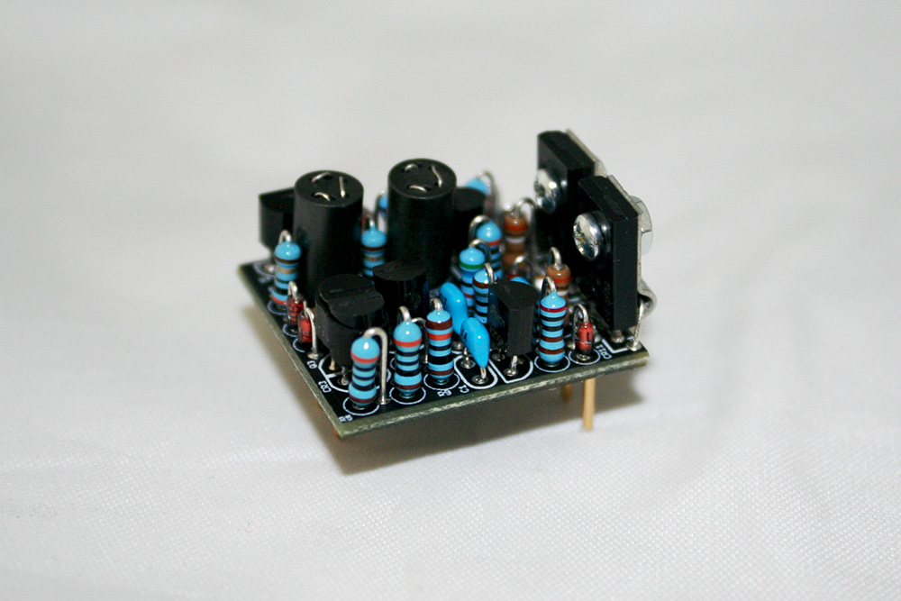
Deane Jensen’s now famous JE-990 paper describing the design, testing, and theory behind a powerful ultra-low noise operation amplifier, was first introduced in the February 1980 AES journal. The design started with the LM394 dual super matched transistor as the input device. The LM394 is a monolithic device consisting of two pairs of 50 transistors connected in parallel to eliminate random variations in the individual devices. In addition to being designed for low noise, the JE-990 is a powerful op-amp capable of
adequately driving a 75Ω load. Many commercial versions of the 990 design are available for purchase today. The John Hardy Co JH-990C+ is certainly the best and most well-respected version. Luckily, it’s also one of the most affordable. Unfortunately, the JH-990 is potted and not very DIY friendly. Many of the other designs available for purchase fall short of the original design and are 990 op-amps in name only.
Shortly after the release of the Lola mic pre, we began offering a DIY JE-990 that would be affordable, authentic, and easy to build. Well, at least as easy as soldering over 30 components on a one-inch square PCB can be. Certainly, it would need to a 2520 footprint and I would need to source an affordable LM394 substitute. Luckily much of this work had been completed a few years ago by PCB designer MNATs when he designed a DIY JE-990 2520 layout. I contacted MNATs about reworking the PCB for a different input component to replace the discontinued LM394 and he agreed to give a shot.
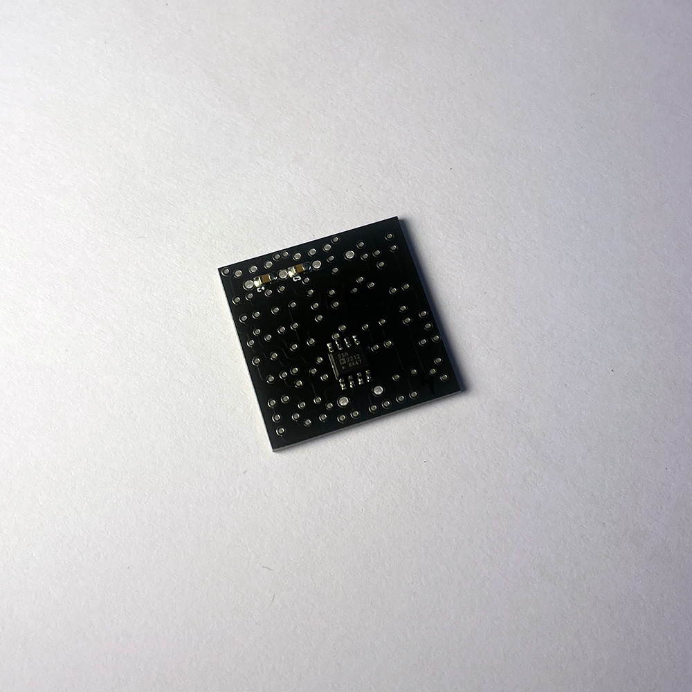
The common replacement for the LM394 is the Analog Devices MAT12. The MAT12 is the successor to the MAT02 and is available in a TO-78 thru-hole package. A very elegant component, but not a cheap or easy to fine. They can cost $35-$100 depending on quantity. Luckily there is another option. Analog devices also offer the SSM2212 which a dual matched transistor surface mount device (SMD) offering even superior performance specs than the LM394 or MAT12. Even better, it can be purchased for a fraction of the cost of the LM394. The Hairball Audio DIY-990 uses this device.
Soldering Guide
Soldering WELL is one of those things that seems easy until you try it. With a small PCB such as the DIY-990, good soldering skills are a must. As always, with solder, less is more. Dave Jones’ of the EEVBlog has created an excellent set of video tutorials. The tutorial is presented in three parts: tools, soldering through hole components, and soldering surface mount components. For our purposes, I recommend you watch part 1 and 2. The videos are lengthy at about 25 minutes each, but they are well worth watching. Even I learned a few things. The videos can be seen by visiting:
https://www.hairballaudio.com/eevblog-solder-tutorials
PCB Overview
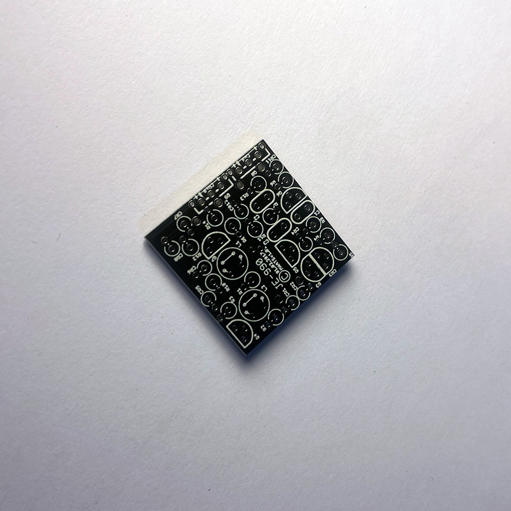
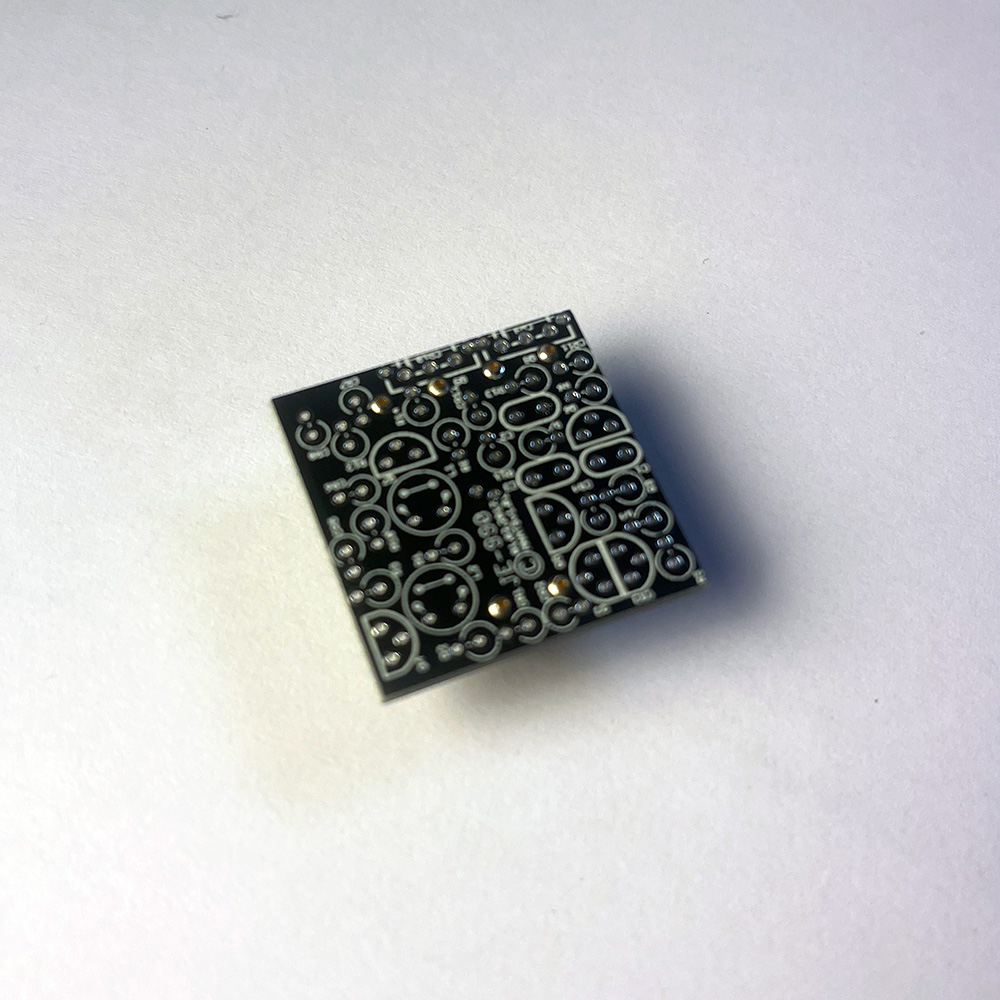
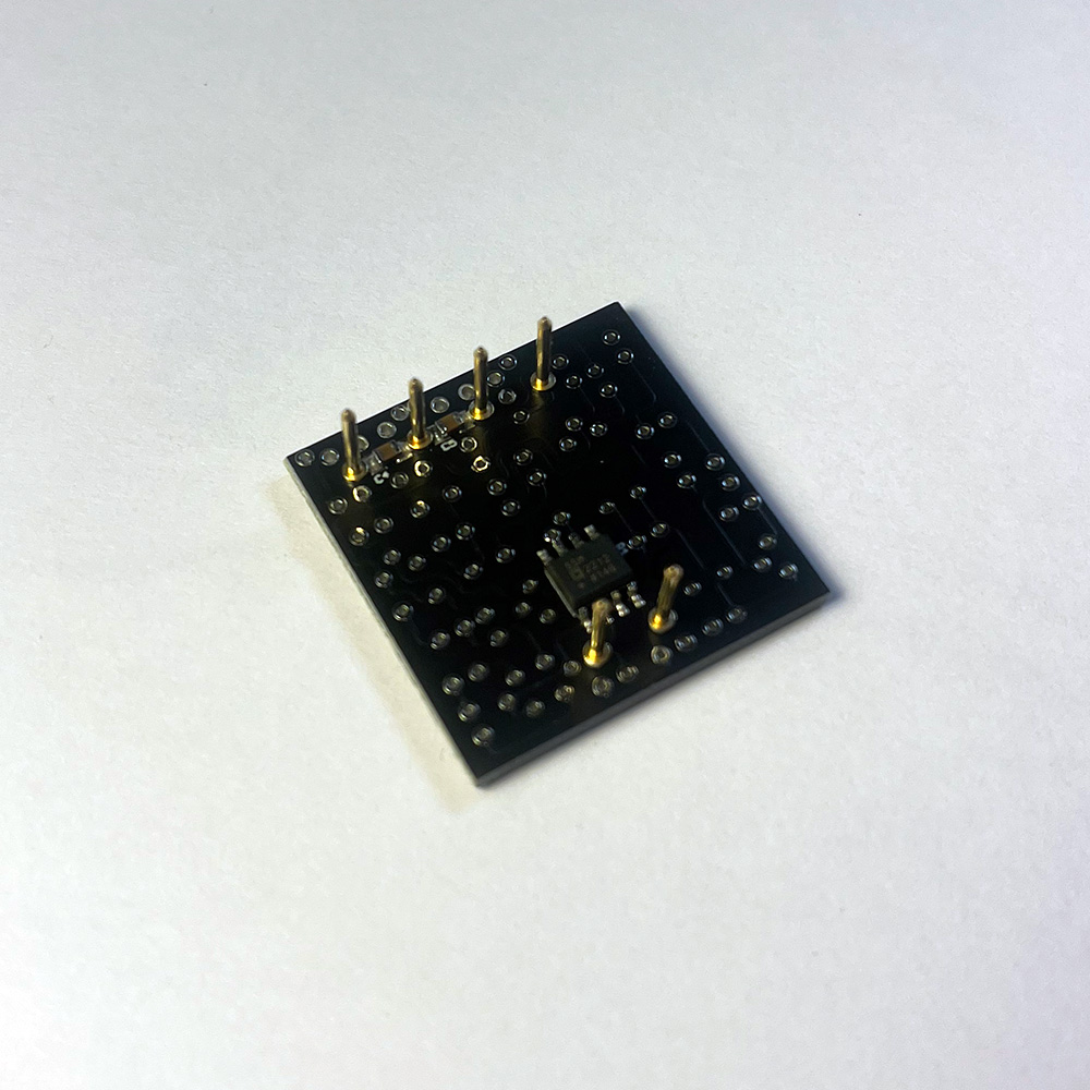
The DIY-990 arrives with the SMD components already installed. Two small 0.1uF SMD bypass capacitors, and the SMD SSM2212 dual surface mount 8 pin transistor. These componets are mounted on the bottom side of the PCB. The remaining components, with exception of the PC pins, are all mounted on the top side.
PC Pins
Start by locating the 6 PC pins in the bag with "Hardware". These are the pins the press into the sockets of your mic pre after assembly. We recommend installing these first since soldering them on the top side of the PCB will be near impossible when the other components are installed. The easiest way to install these pins is to press them fully into the sockets of your mic pre or device that will use these op-amps.
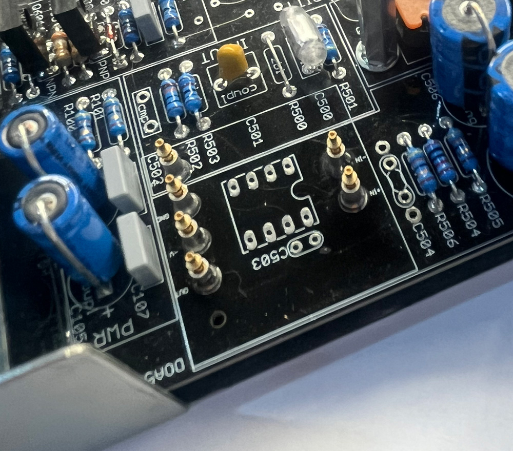
Now you can align the PCB holes for PC pins and press down. The SMD parts should be facing down towards the PCB.
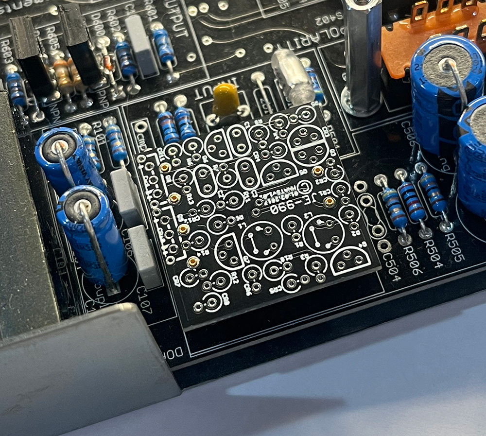
This is the one component you will apply solder on the top side. A little solder goes along way, try to avoid a big blob. Heat the top side of the pin and PCB and solder in place. If the solder on either side of the two bottom side SMD caps interferes with the pin sitting fully flush to the bottom of the PCB, simply start soldering the pin and it will melt the bottom side solder and sink into place.
Diodes
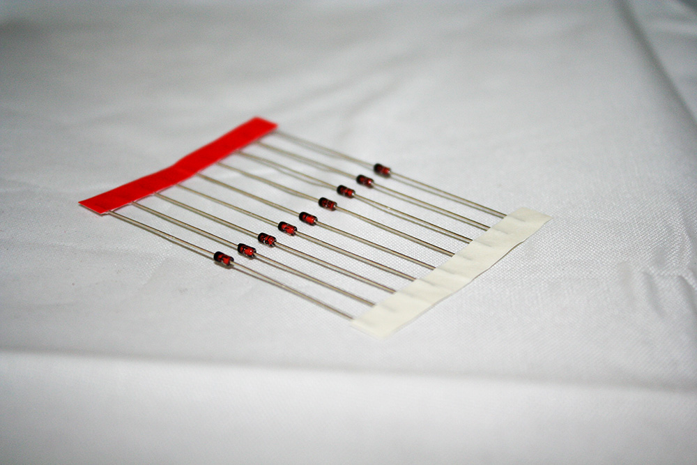
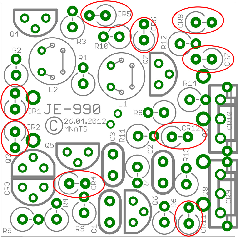
Start by installing the nine 1N914B diodes that are located in the DIODE/TRANSISTORS/CAPCITORS bag. These diodes, along with the resistors you’ll install in the next step, are mounted vertically on the PCB.
Note that the cathode side of the diodes are labeled with a black stripe. Bend the OPPOSITE lead back towards the body of the diode.
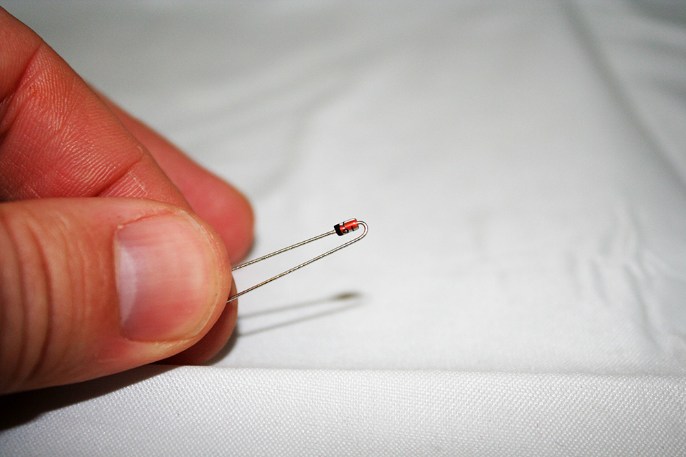
Diodes are POLARIZED devices. They must be mounted in the right direction. For the DIY-990 PCB all diodes are mounded so the cathode, the end with the black stripe, meets the side of the component footprint with the circle around the pad.
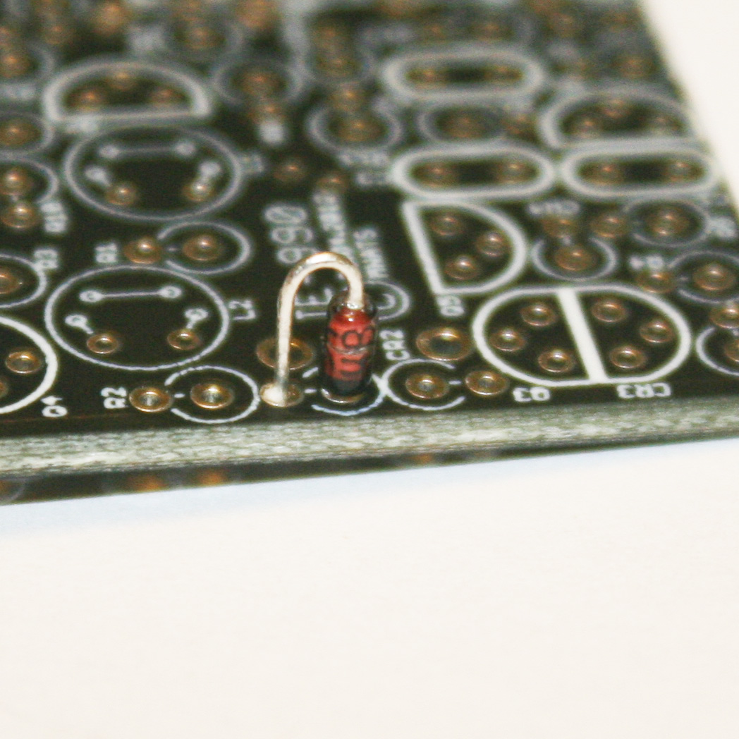
The next page shows where these diodes should be placed. When you’re done you should have something that looks like the image below.
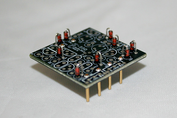
Diode Map
Resistors
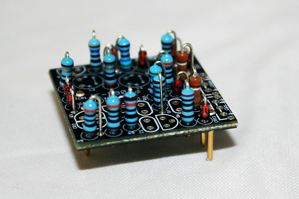
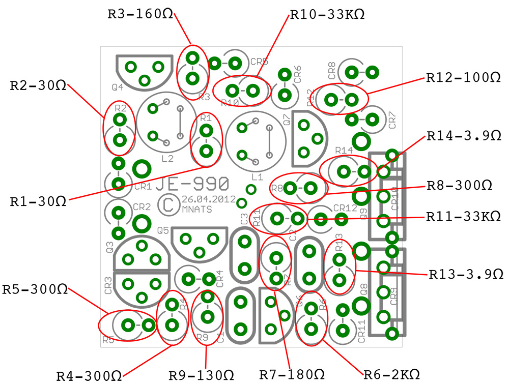
Next, you’ll install the 14 resistors. Check each resistor with a DMM and sort them. Although the resistors are not polarized, to avoid leads touching and shorting, you should install them so that the body meets the side of the component footprint with the circle around the pad.
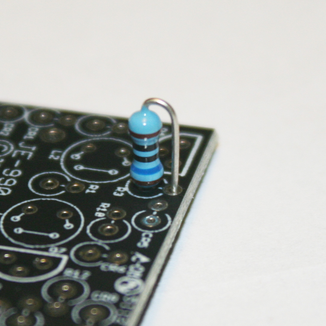
The next page shows where these resistors should be placed. When you’re done you should have something that looks like the image below.
Resistor Map
Capacitors
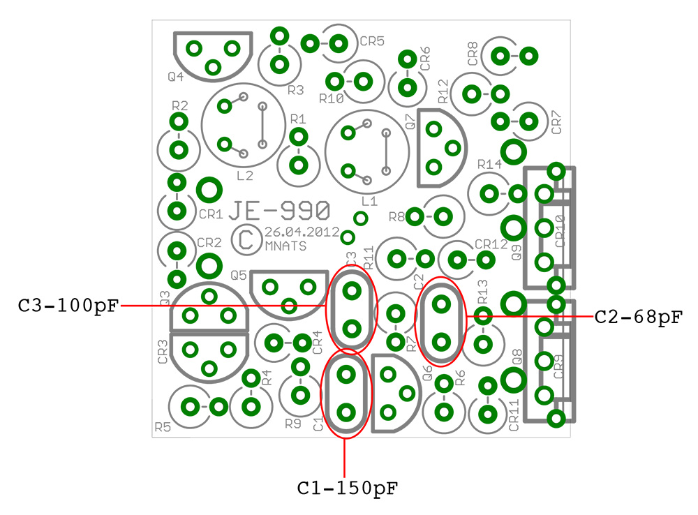
Next, you’ll install the three ceramic caps. These are non-polarized and can be installed in either direction. However, you must install the correct value in the proper place.
To determine the capacitor values, look closely at the capacitor body. On one side you’ll see numbers followed by the letter “J”. The first two numbers set the value, the third sets the multiplier, and the J indicates a 5% tolerance. For the DIY-990 the values are as follows:
68J = 68pF
101J = 100pF
151J = 150pF
The map below shows where these capacitors should be placed. When you’re done you should have something that looks like the image below.
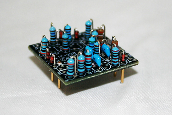
Capacitor Map
TO-92 Type Transistors
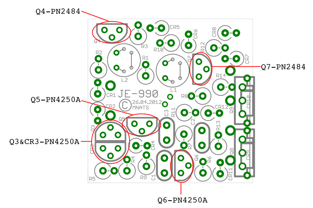
Next, you’ll install the TO-92 transistors. There are four PN250A and two PN2484 transistors. You can identify them by looking at the identification marks on the flat face of the body.
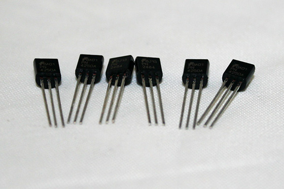
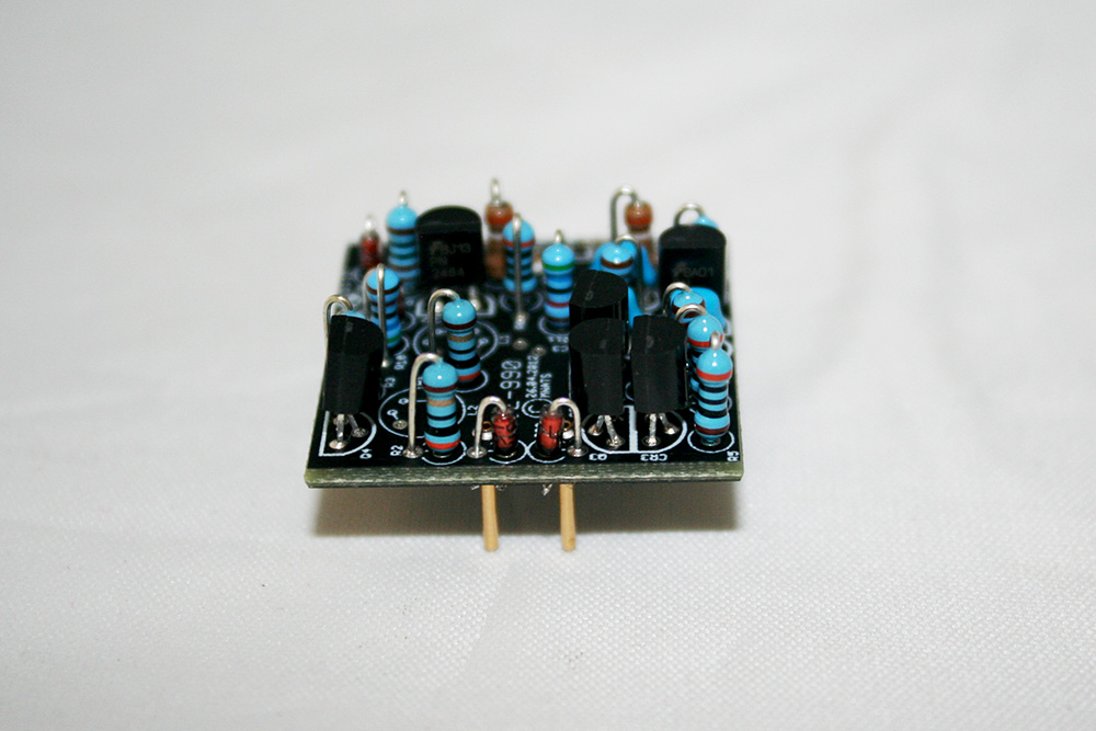
CR3, though a diode designation, is a PN4250A transistor connected as a diode. This allows us to bond the body faces of CR3 and Q3 for thermal coupling as instructed in the AES paper. Before installing these components place the supplied shirk wrap tubing over the transistors and shrink it with a heat gun or hair dryer.
Transistor Map
Output Transistors and Diodes
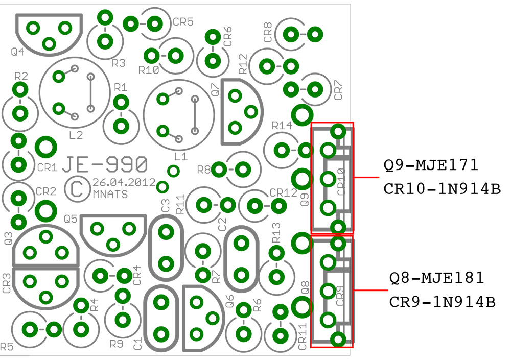
The TO-220 type output transistors (Q8 & Q9) must have 1N914B diodes thermally coupled to their bodies to prevent distortion with low-impedance loads. This is achieved by using the supplied clamp. Looking at the PCB silkscreen, you’ll see that the cathode (black stripe) should be facing right when viewing the TO-220 transistors from the rear (side with metal tab). This is true for both the MJE171 and MJE181.
THREE IMPORTANT POINTS!!!
1. These transistors are not the identical. The transistor marked MJE171 is a PNP transistor and needs to be placed in the Q9 footprint and one marked MJE181 in an NPN transistor and needs to be placed in the Q8 footprint.
2. The cathode of the diode (side with the black line) must be on the right side on both the MJE171 and MJE181 when looking from the back. See the image below. Having the diode facing the wrong way is the number one error in these builds.
3. When you clip the diode to the transistor, ensure the diode leads are not touching the clamp or the diode may short across the metal clamp and not perform its function. You can use the transistor body as a jig for bending the diode leads.
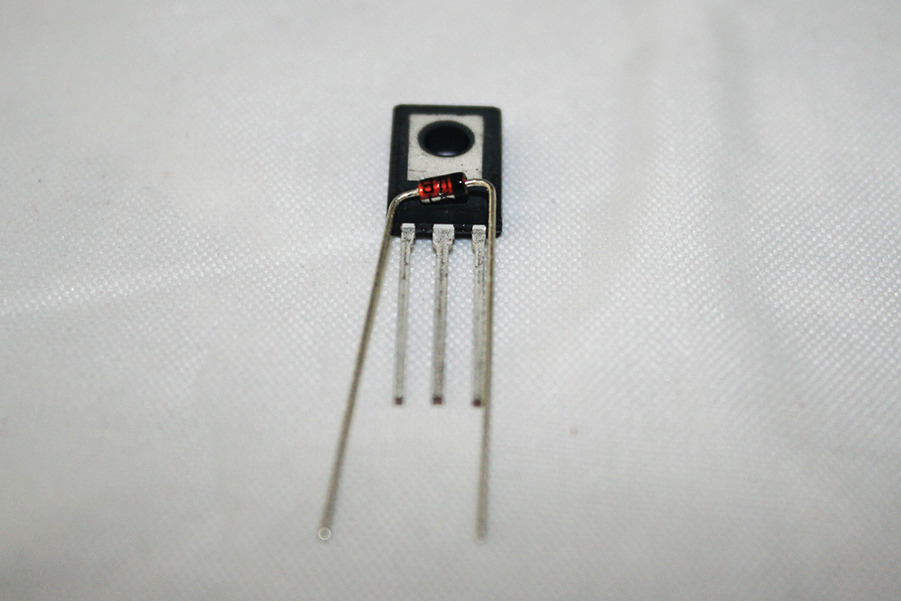
The bottom edge of the clamp wraps around the diode and extends just past the transistor mounting surface fitting snug to the transistor bottom. Center the clip, which should sit flush to the surface, and use the supplied #2 screw and nut to secure the clamp. The pads for the inner leads of each diode are very close on the PCB and may become bridged with solder or make contact. This is ok, they are connected on the circuit.
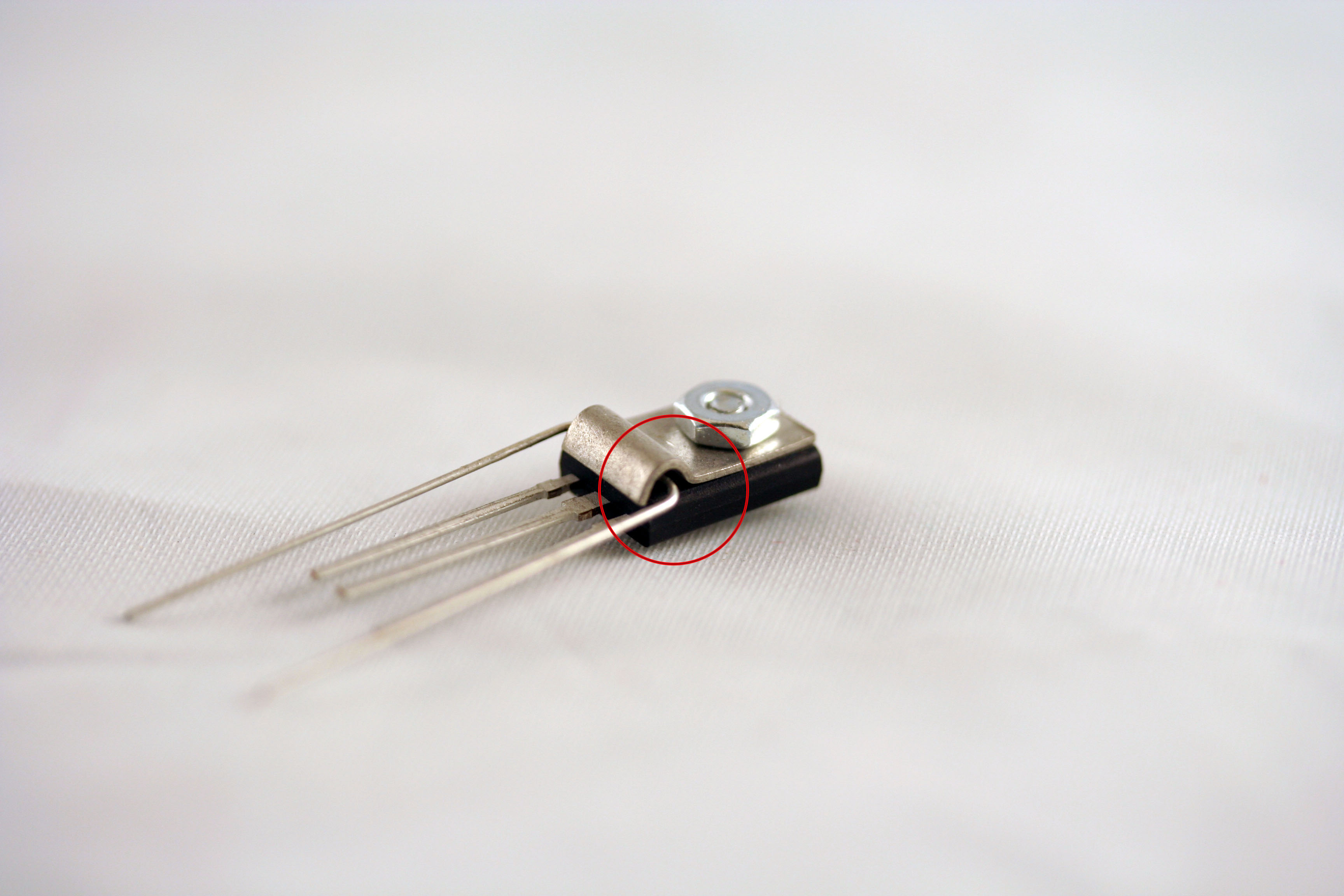
Note the red circle: The diode leg is clear of the clamp
Output Transistor and Diode Map
Inductors
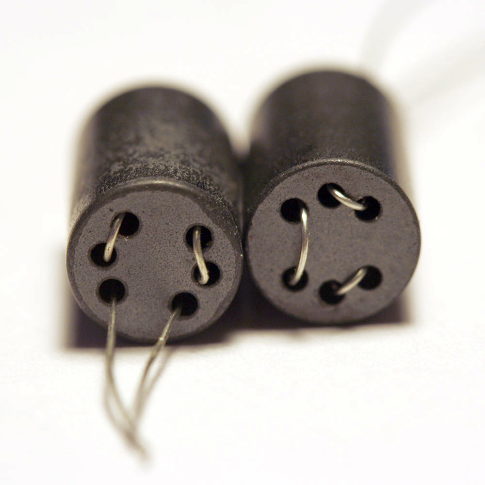
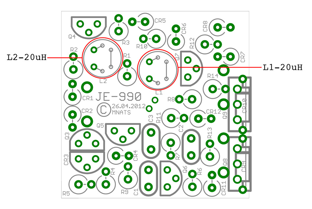
The two 20uH inductors are often missed in many 990 designs. Included are two Jensen inductors you will wind with the supplied 30 AWG wire as described in the AES paper. Winding is simple, there is no top or bottom side, just six holes in two rows of three. You can start at either end of the two rows, below I have started in the upper right. Cut about 8” of wire from your supplied spool then follow the numbers in order to complete the pattern. Pull the wire through slowly and try to avoiding kinking or leaving it too lose. Do not pull too tight, or the wire will break. We’ve supplied some extra wire for just in case.
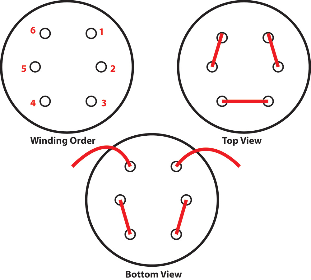
Inductor Map
Final Thoughts
You’re done! Congratulations, you've built a JE-990 to the specifications of the famous Jensen AES paper. All that’s left is to insert it into you circuit or design a circuit around it. It will happily run on +/- 15-24 VDC supply.
