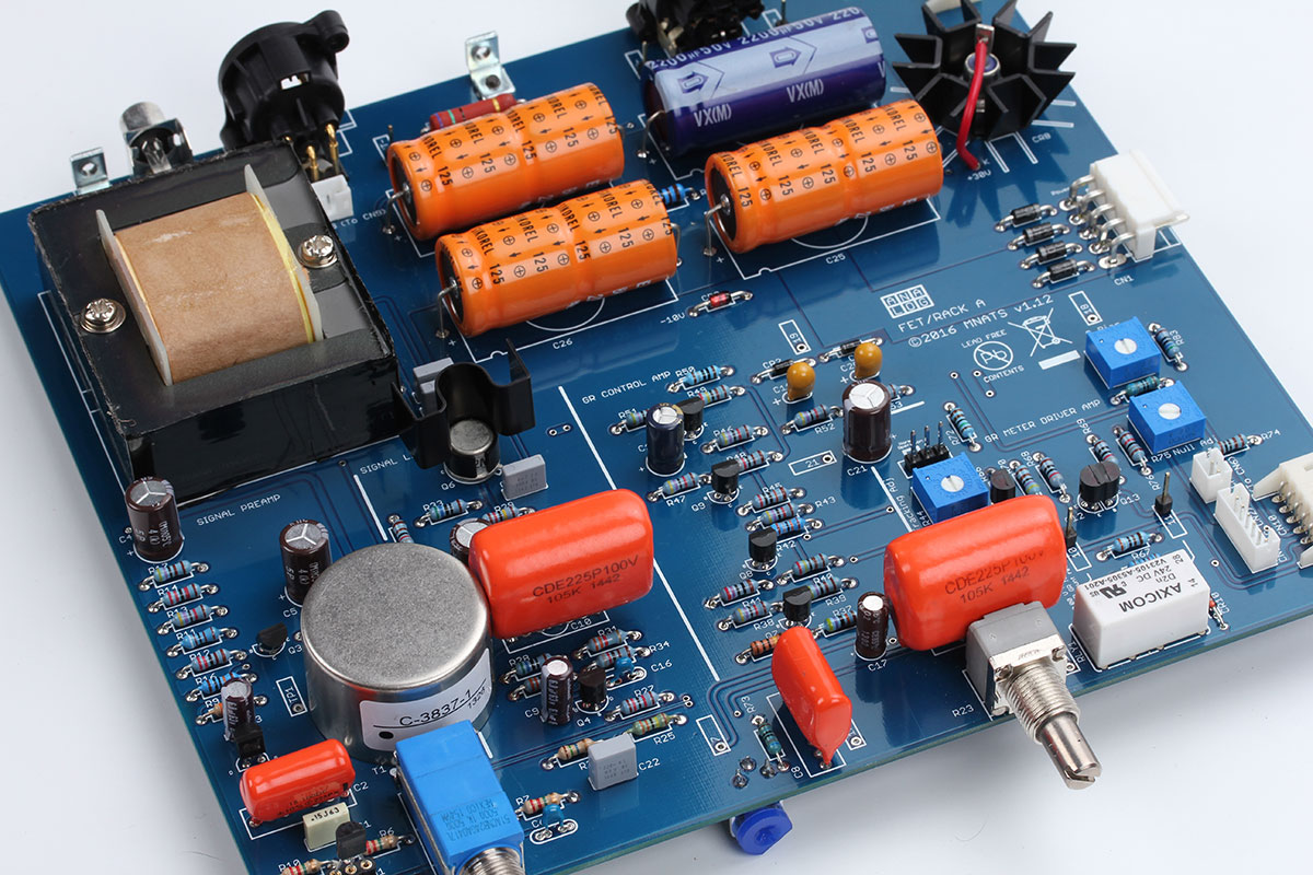
Populating the Main PCB
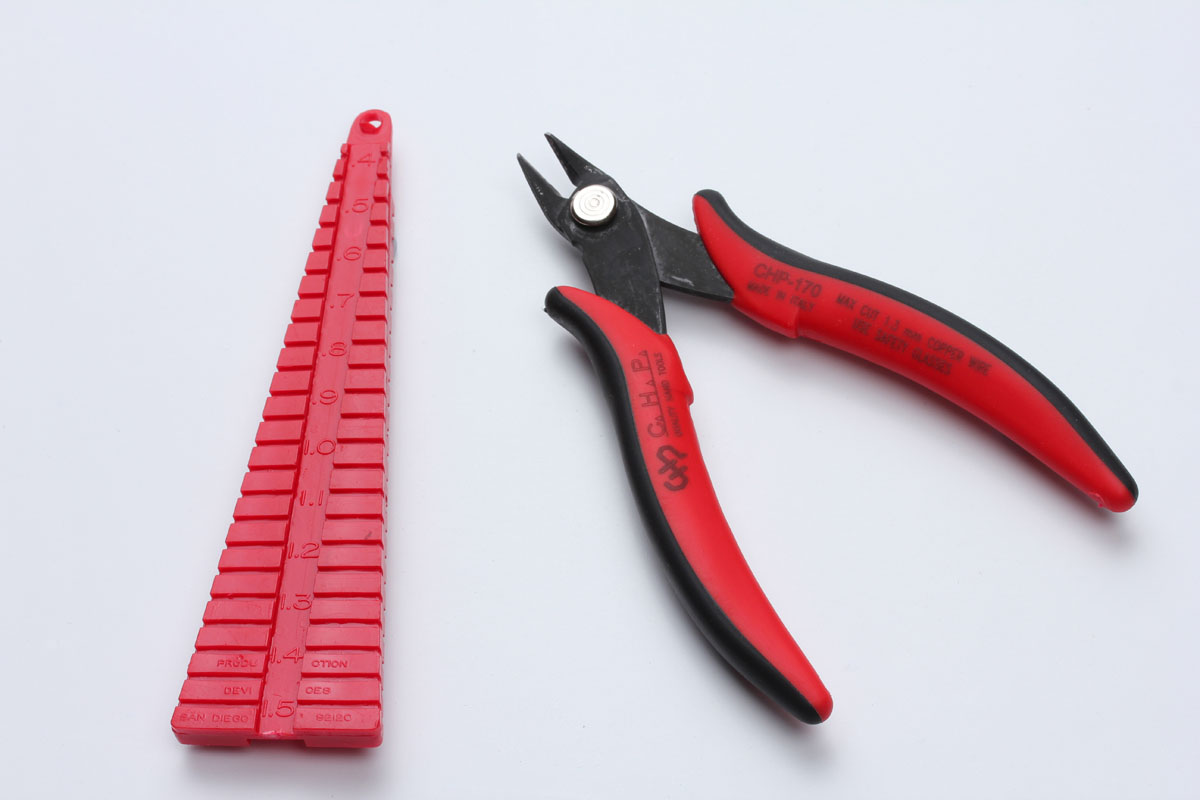
Now that your power supply is built and tested, you can proceed with populating the rest of the PCBs. Start by printing the parts list or opening up the online PCB stuffing map. I like to cross out each component as it's soldered into place when using a printed guide. In addition to a soldering iron and a digital multimeter (DMM), you’ll need some decent lead trimmers and a lead bender or needle-nose pliers. This lead bender is Mouser part 5166-801.
Enough! Let’s populate!
Diodes
PCBs are generally populated by starting with the smaller components that sit closest to the PCB and ending with the larger components. The diodes are as good a place as any to start. There are a few different types in the FET/RACK. The 1N2989B stud diode and four 1N4004 diodes you've already installed in the power supply section. Your diode will have its name (FDH333, 1N4004, 1N914..) printed on the diode itself. Look really close! There may be other numbers and letters on the parts that we don't refer to in the guide. You can ignore these, they are typically tolerance or date and place of manufacture codes.
It's important to note that regardless of the type, diodes are polarized devices. Specifically, they have a positive (anode) and negative (cathode) lead. They must be inserted properly to work. On the diode, you will notice one lead is marked with a line. This line indicates the negative or cathode lead. The silkscreen also shows the diode with a line at one side. This indicates how the diode should be inserted. Pretty easy!
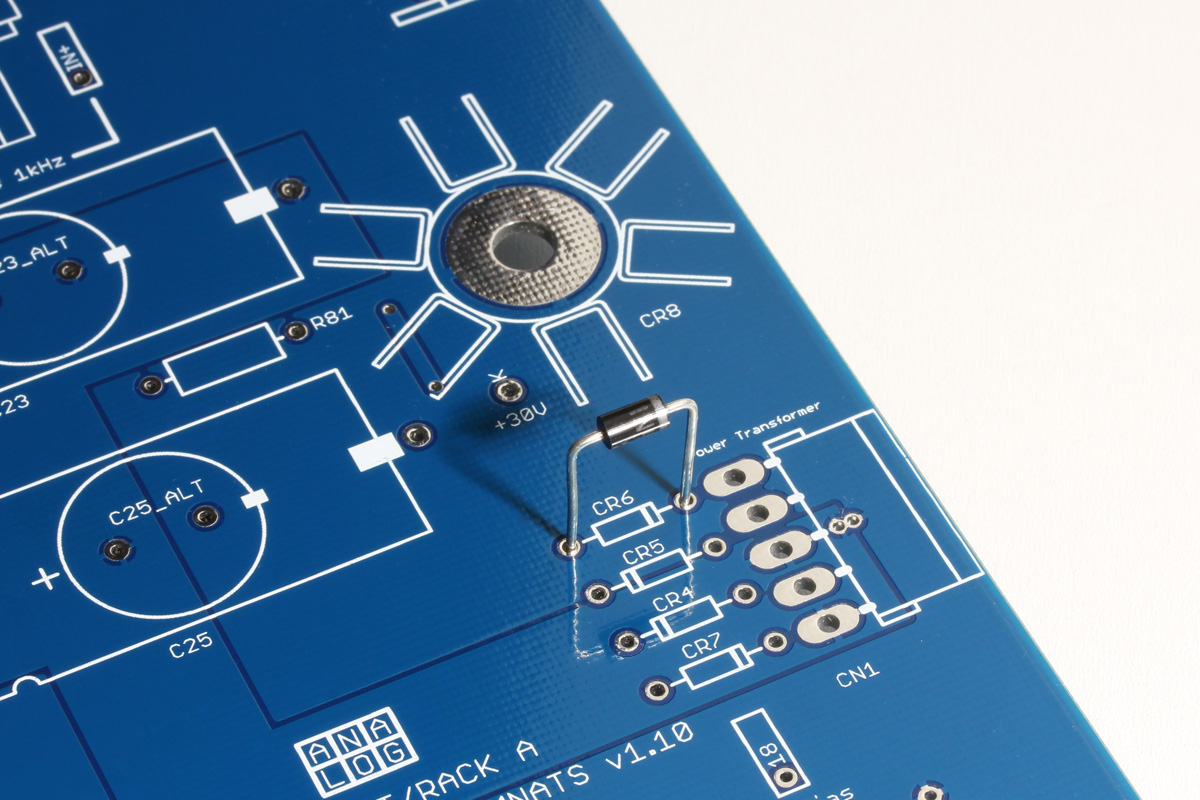
If you have a lead bender, start by bending the leads to match the PCB spacing or "pitch".

Notice how the line on the diode (cathode lead) is on the same side as the line on the silkscreen layer in the image below.
All parts, unless specifically noted, should fit tightly and flush to the PCB. We service about 50 different builds per year and the single biggest issue across all products is poor soldering and components hanging off the PCB. Let's examine how to properly solder your components so they fit tightly to the PCB and give you the best chance at a good solder joint.
Start by pushing the part down against the PCB. Flip the PCB while holding the component in place and bend the leads at a 45-degree angle. You can pull a little and bend to make sure the component is tight to the PCB. Now the part is held in place by the bend and your component will not slip down.
Now that the component is securely in place, there's one last issue. The long thick leads will act as a heat sink as you try to solder the component. Since they need to be trimmed eventually, now is a great time to do that. Trim them just above the PCB making sure not to cut away the bend holding it in place.

With the part in place and the leads trimmed, you're ready to solder using the appropriate solder technique explained in the linked video at the start of this guide. Note the soldered joint below. There is an appropriate amount of solder, not a huge ball. You want to use just enough solder to fill the thru-hole and form a small shiny fillet.
Take your time installing and orienting the rest of your diodes.

Resistors
Time to grab a beer, brew a coffee, or put on your favorite record. This one will take a while. Take your time, misplacing a 270Ω for a 270KΩ resistor is not an easy mistake to sort out when your build doesn’t work right. It helps to test each resistor with your DMM Ohm (Ω) setting before soldering it in place. You'll rest easy later on.
It's important to note, however, that not all meters are created equal. Even great meters do not measure high resistance or very low resistance accurately. Everything has a resistance/impedance, including your meter reading input. When measuring a resistor, its input resistance is in parallel with the resistor under test. For practical purposes, low input resistance meters (1M) will measure resistors 10K or above as having a lower resistance. Meters with higher (10M<) resistance will read accurately into the megaohms but still have their limitations (3Mohms or higher).
Measuring lower resistance is problematic because your meter leads themselves have resistance. Resistors under 10Ω may measure a few ohms higher from added lead resistance.
It should be noted that resistors are rarely defective out of the box. If you read the color codes, you'll only need the meter to double-check. Just be aware that at higher resistance your values may measure lower. It's your meter.
Digikey.com has a great calculator tool to help you with color codes. Most of the resistors in the kit are 5 band blue metal film resistors.
The larger values are the beige carbon comp 4 band resistors.
Important!
PCBs V2.0 and higher have R-OPT on the mainboard by the input t-pad. It is NOT supplied with the kit. It's an optional mod to tame the input if you feel you need it. You can use any 100Ω resistor 1/8W or higher that will fit. Details can be found on the input mod page. If you're not using the mod, leave that space empty. The revision A has another R-OPT on the ratio PCB. It is a 10MΩ resistor and is supplied with your kit. You should install it. It is a resistor that will prevent a popping sound when switching ratios. It was added to the Rev C and beyond. If you want to be 100% authentic to the Rev A, you can leave it empty.
To stuff the resistors follow the diode stuffing steps above. The only difference being resistors are not polarized and can be inserted in either direction. For troubleshooting purposes, we suggest that you align the resistors so all of the color codes read in one direction on the horizontal and vertical plane. This will make double-checking values easier should you need to troubleshoot.
Your PCB should now look like the image below. Good work!

Note: The Revision A includes an optional 10M resistor on the ratio PCB (R-OPT). This resistor was not in the original Revision A, but was added to later revisions to prevent audible pops when switching ratios.
Transistors
We could go a few different directions at this point, but let's move to transistors. These have three leads. The majority of the transistors in the FET/RACK Compressor are actually not FETs, but BJTs or Bipolar Junction Transistors. These have a collector, an emitter, and a base. These can vary from component to component so to make it easy for you, the PCB silk-screen matches the package of the transistors. Most are T0-92 packages that look like a “D” from the top and align with the “D” on the silk-screen.
![]()
The first three transistors above are TO-92 package transistors and the last one is a round TO-39 transistor (Rev A and D only). You can see on the TO-92 transistors that the part name is on the lower half of the flat face. The upper half contains the manufacturer name and date codes that can be ignored.
Q1 and Q11 are the FETs of the FET Compressor (The Rev A also has some J309 FETs). Q1 is the compression FET and Q11 controls the meters GR display. These FET leads are named source, drain, and gate and are TO-92 types (D-shaped). These FETs have their transfer curve matched to within 10% to ensure your meter and the actual GR are the same. You’d be surprised how widely transistors can vary out of the same box. Luckily these arrive matched for you.
Having the option to remove or change the Q1 and Q11 FETs can be a valuable troubleshooting option. Though not included in the kit, you can opt to install sockets in these two positions to make removal very easy. Note that the sockets are soldered to the PCB, the transistor are pushed into the sockets and soldered.

The remaining transistors, including Q1 and Q11 if you're not supplying sockets, can be soldered directly to the PCB. They should sit just above the PCB as shown. Note the orientation in relation to the silkscreen. Transistors (and diodes) are very sensitive to static electricity and excessive heat. Try to keep this in mind while installing these components.

On Rev A and D circuits, Q12 and Q13 should also be matched for Hfe (gain) and will arrive matched. The matched pair will be taped together. These transistors face one another and should touch on the flat side for thermal coupling.
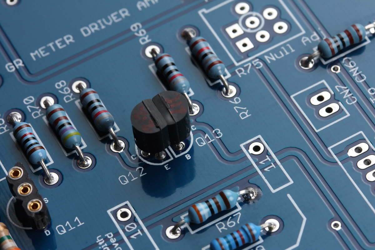
The rev F circuit uses a TL071 IC in place of these transistors, so matching is not needed.
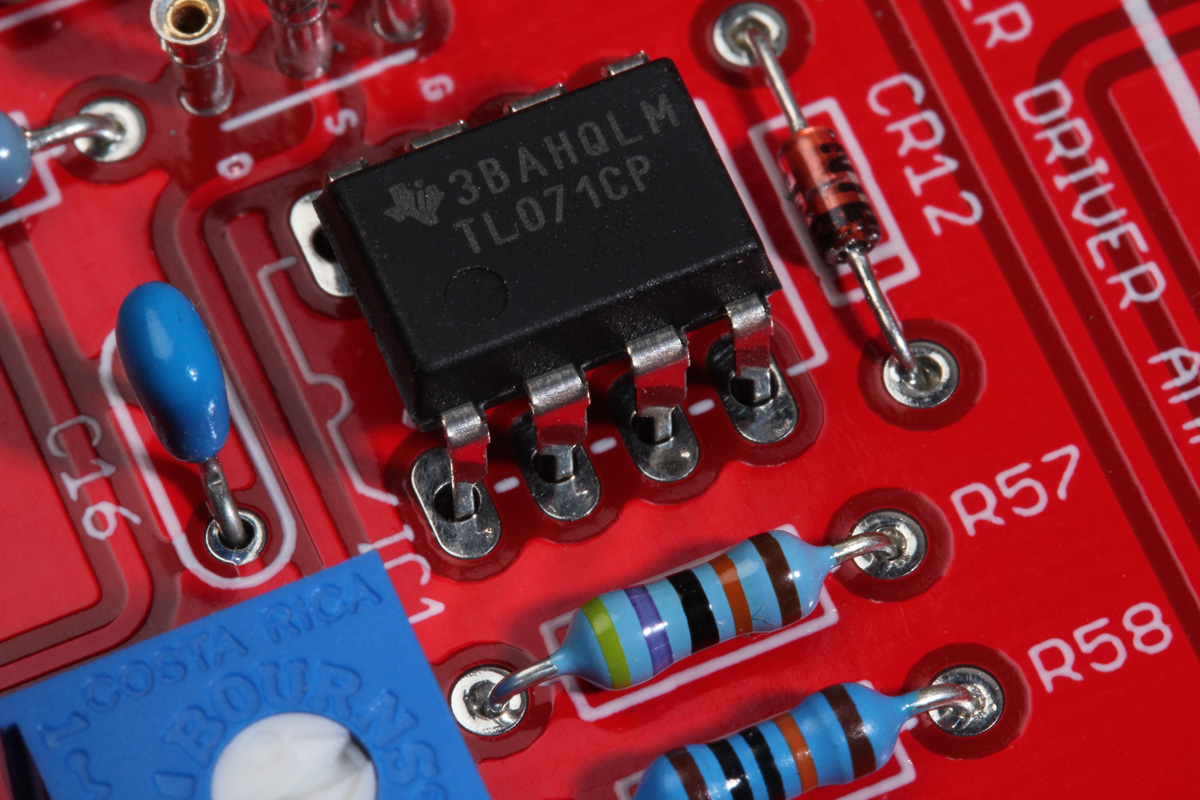
The TL071 must be inserted in the correct direction. Note the circle indent on the surface of the IC indicates Pin1. That circle should be oriented with the semi-circle on the PCB silkscreen footprint.
The Rev A and D also have a TO-39 transistor (2N3053) labeled Q6 which has a tab that should line up with the silkscreen tab. It comes with a small black plastic standoff to fit between the transistor and the PCB. This allows it to sit a little above the PCB and dissipate heat, while still keeping the leads stable.
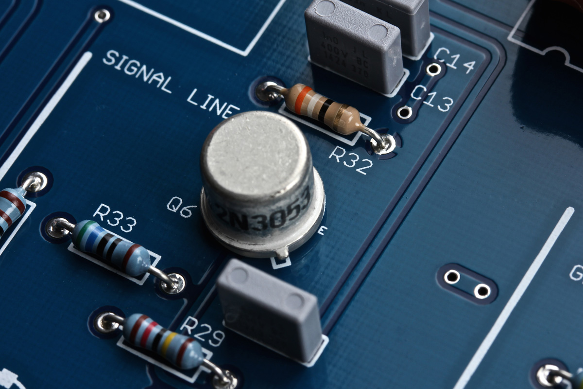
This output transistor also needs to have a heatsink (supplied) slipped onto it to avoid thermal runoff. This part gets hot! You may want to wait until the board is fully stuffed to add the heatsink but be sure not to forget it!
Starting with the rev F, the output circuit was changed from class A to class A/B. Rather than one output transistor that gets really hot, the rev F has an output transistor pair that stay cool.
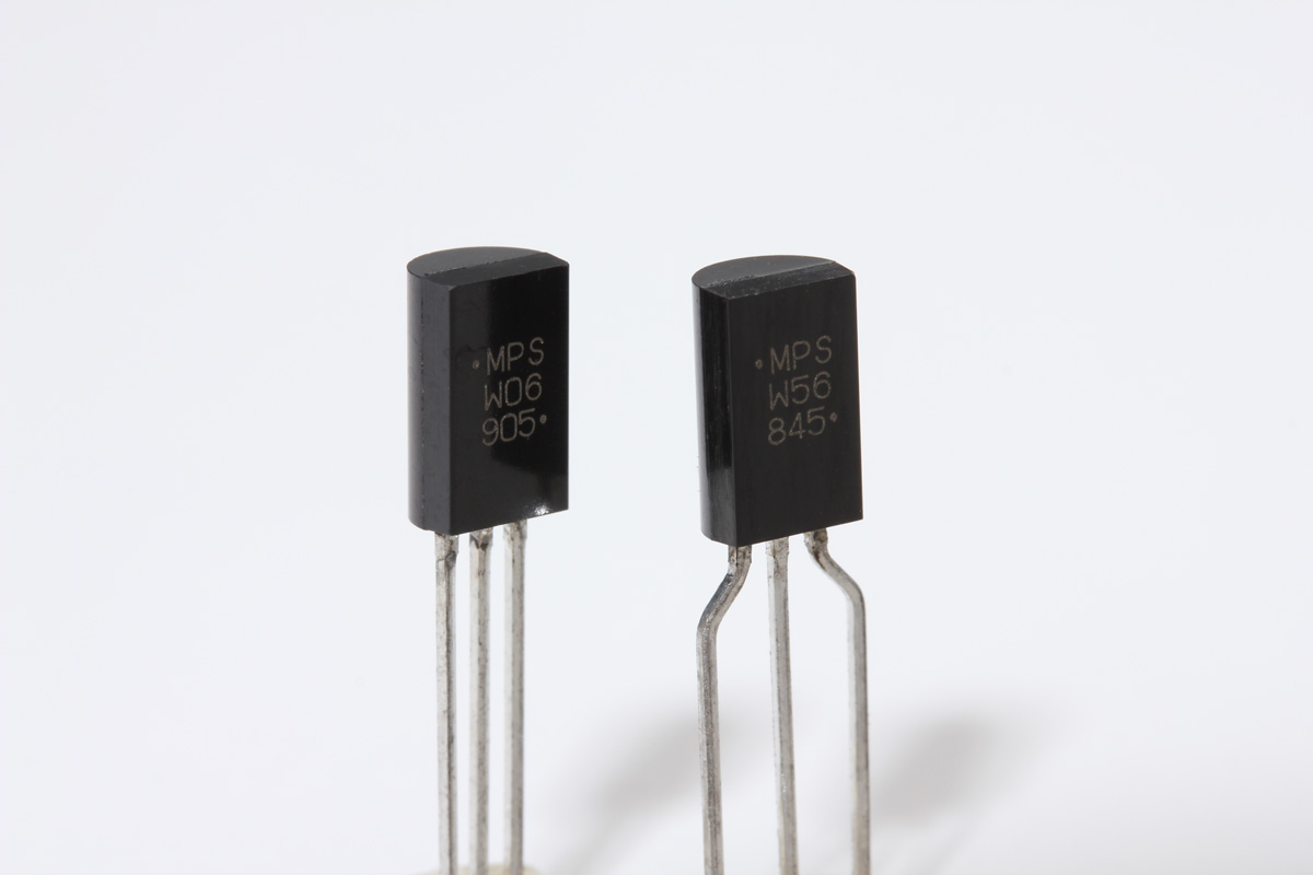
This rev F output pair (MPSW06 and MPSW56) are tall TO-92 transistors. They are installed like other TO-92 transistors and require no heatsink. If your transistors arrive with kinked leads you may have to straighten them with pliers for easier installation.
![]()
Trim Pots
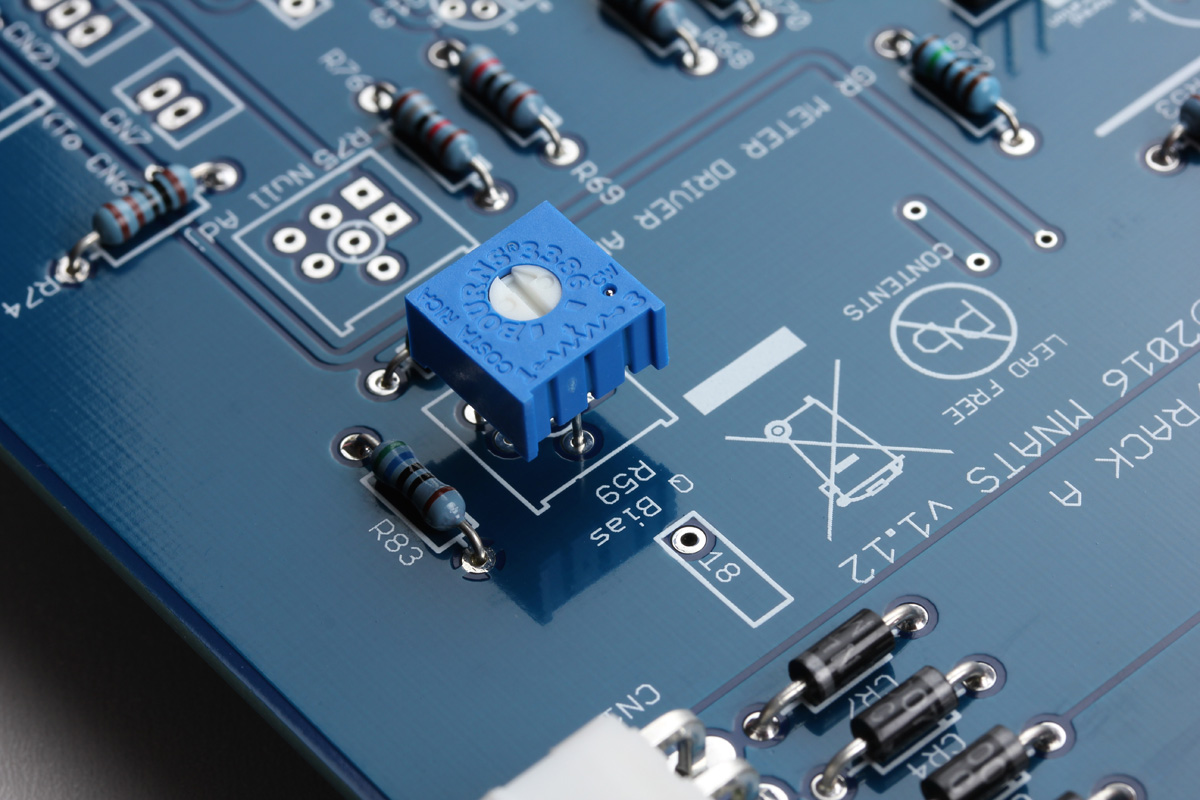
Let’s talk trim pots. The trim pot is essentially a variable resistor. It has three legs. If it’s a 2K trim pot, there is 2KΩ of resistance between the two outer leads. The middle lead, the wiper, slides back and forth between them and is controlled by the screw adjustment. If the wiper is rotated all the way right, there will be near 0Ω resistance between the wiper and the right lead and near 2KΩ between the wiper and the left lead. Rotate it all the way to the other side and they will be opposite. These are variable resistors used to calibrate various circuits in your FET/RACK.
The value of each trimmer is noted on the component. The first two digits are the first two numbers of the resistance in ohms and the last digit is the multiplier.
101 = 100Ω
202 = 2KΩ
104 = 100KΩ
Of course, you can always double-check the value by measuring the resistance between the two outer leads with your meter.
Let's mount them on the PCB. There are 7 pads for each trimmer. These allow for alternate trimmers for those that like to source their own parts. The trimmer supplied can only be inserted one way and should match the silkscreen.
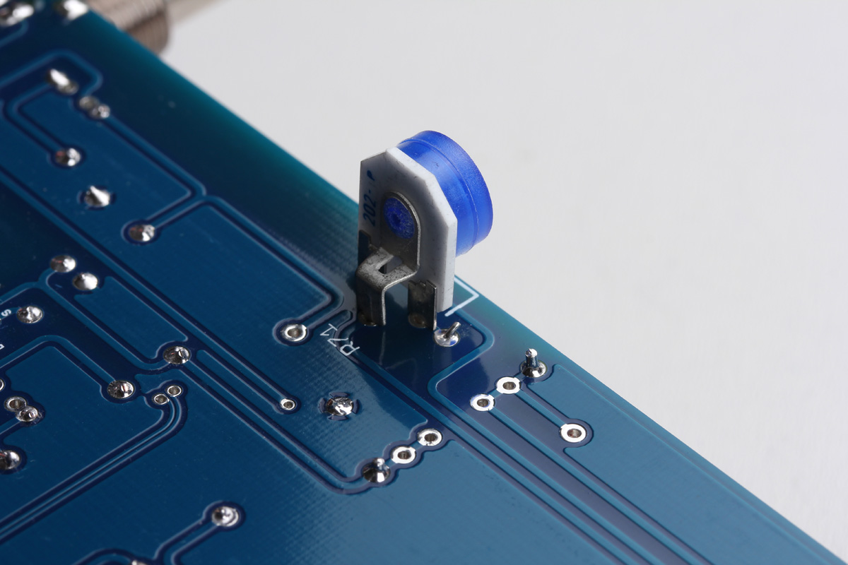
There is also a 2K zero adjust trimmer (R71). This adjustment is made through a hole on the front panel that sits between the input and output knobs. It is mounted on the bottom side of the PCB. You may choose to leave this out until you've stuffed the rest of the board as having it protrude from the bottom may make mounting other parts more difficult. Just don't forget it!
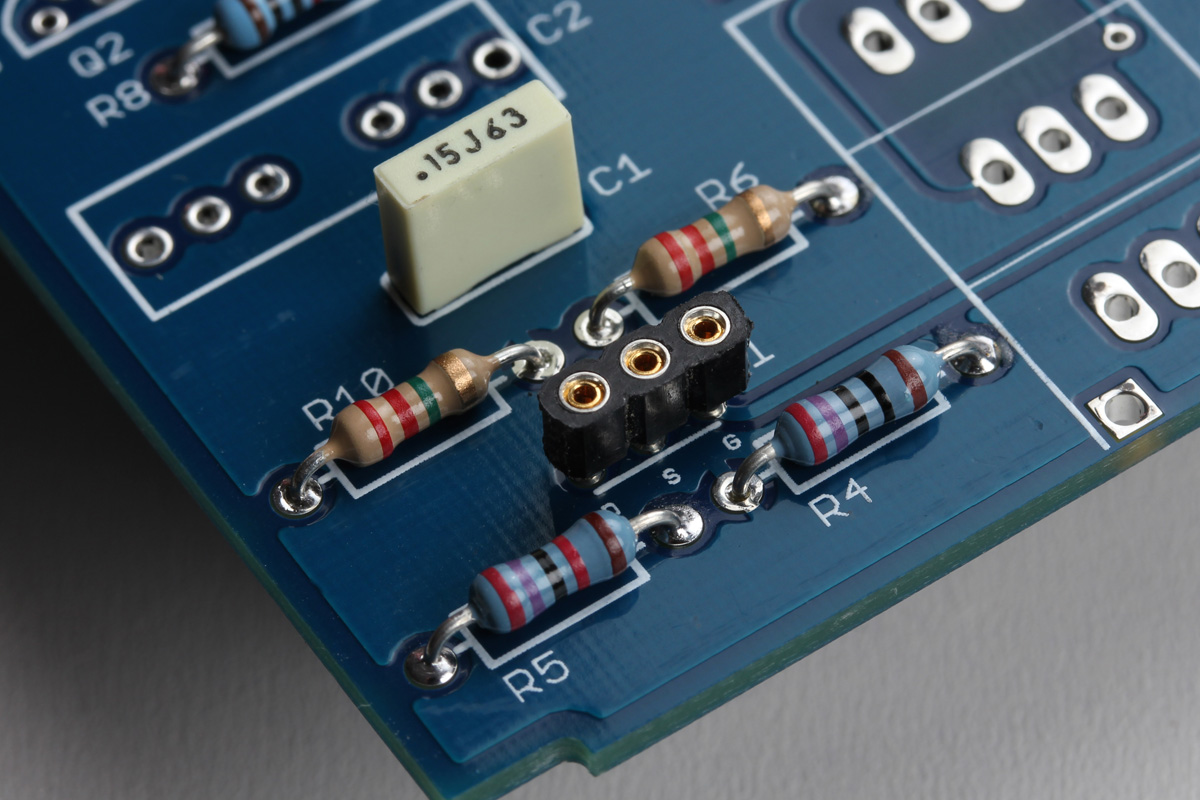
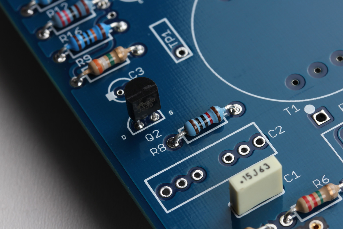
Capacitors
Capacitors (caps) are very cool, flavourful, and play an important role in your build.

Shown above are the types you'll use in your kit. The electrolytic and tantalum capacitors are polarized and must be inserted in the correct direction. The film and ceramic capacitors are not polarized. The larger "Orange Drop" capacitors are also film and only found in the Rev A kit.
The smaller blue ceramic caps have three numbers indicating their value in pF. They are VERY hard to see, but they are on there. Look close in good light. The first two digits are values and the third is the multiplier.
Example:
100 = 10pF
330 = 33pF
201 = 200pF
Capacitors smaller than 10pF will be labeled with an R in the decimal place and have no multiplier:
6R8 = 6.8pF
Note that using the capacitance measurement on your meter will not work well with these capacitors. Your meter probes and meter inputs have enough capacitance to significantly raise the measurement of caps in the pF range. Trust the printing on the capacitor.
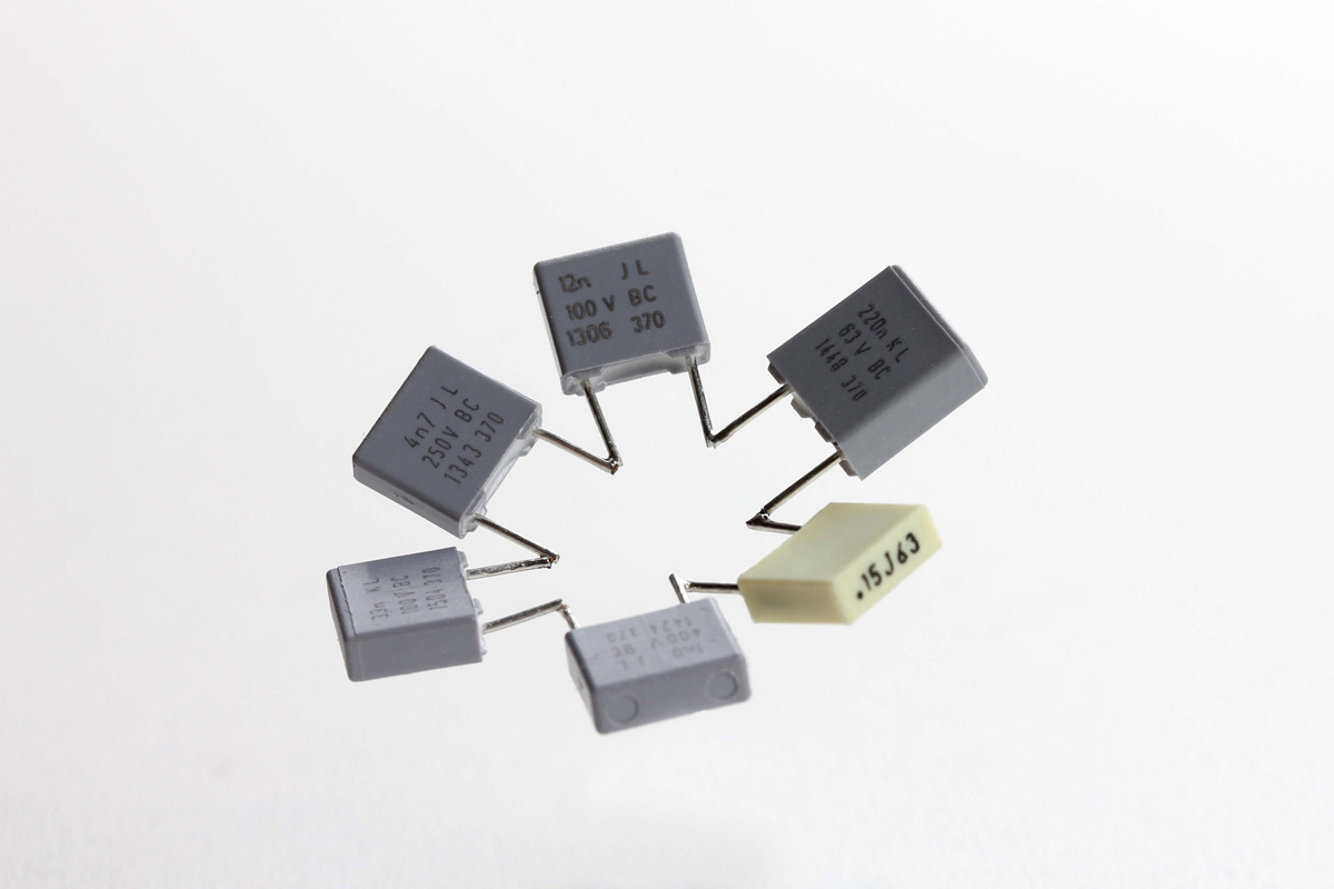
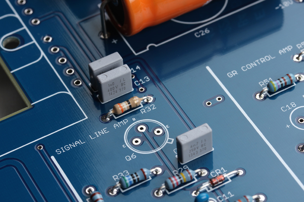
The film and ceramic capacitors are non-polarized and can be inserted in either direction. Our film caps are grey or cream colored. Identifying the value can be a little tricky. Note that film caps generally range in value from 0.001uF up to 1uF. The grey caps tend to show their value in nanoFarads (nF). To convert nF to uF move the decimal three places to the left.
Example:
33n = 33nF = 0.033uF
4n7 = 4.7nF = 0.0047uF
1n = 1nF = 0.001uF
220n = 220nF = 0.22uF
22n = 22nF = 0.022uF
The cream caps usually just indicate the uF value. So 1 = 1uF and .15 = 0.15uF. Ignore letters like J and K and the numbers after them. They are generally tolerance and date codes.
These are mounted like any other component, pulled tight to the PCB with leads bent then trimmed.
The small blue ceramics will sit slightly above the PCB naturally.
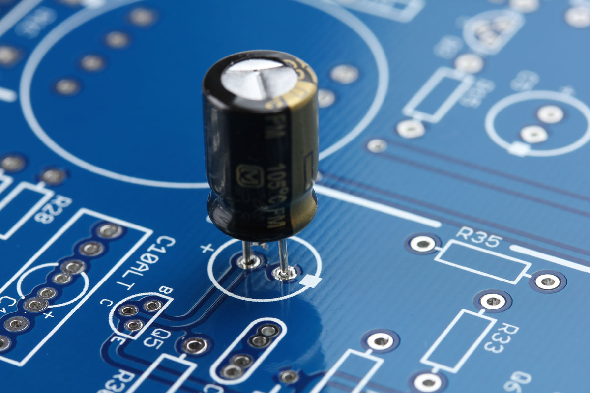
One important note is that the two 6.8uF tantalum capacitors should be used in the gain reduction amp designations C19 and C20. They are polarized and the positive lead is marked with a black line and a +. This lead should be entered into the pad marked “+” on the C19/C20 silkscreen.
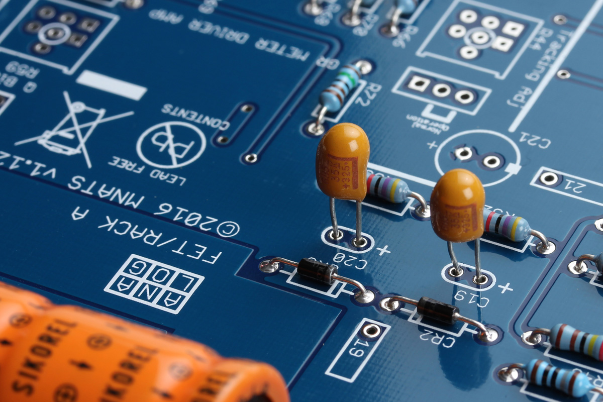
Electrolytics are also polarized. Like diodes, they have a negative lead that is marked. The opposite and unmarked longer lead is positive and it is placed into the pad on the silk-screen marked with a “+”.
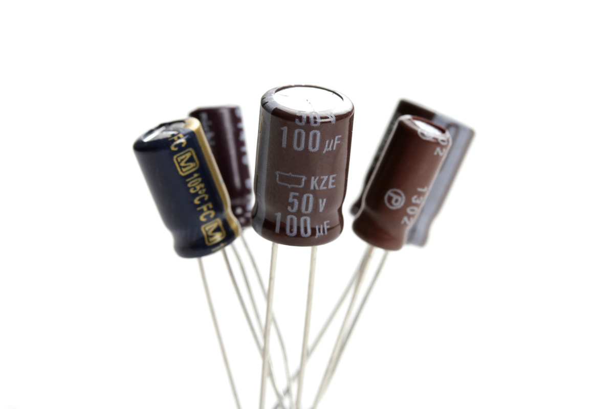
The electrolytic will have their negative lead marked and the positive lead will be longer. The corresponding footprint will have a white box negative symbol on one side and a small "+" mark on the other. Insert them paying close attention to orientation.
Much of your PCB should now be stuffed, but take your time! We've still got work to do.

Some footprints have extra pads for wider capacitors. Make sure regardless of width your capacitor, they should be installed centered on the footprint.
Four film capacitors in the Rev A build are large "Orange Drop" types. C2/C8 are the smaller 0.15uF capacitors and C7/C10 are the larger 1uF capacitors. You may choose to wait to install these at the end, as they add a lot of bulk to your PCB.
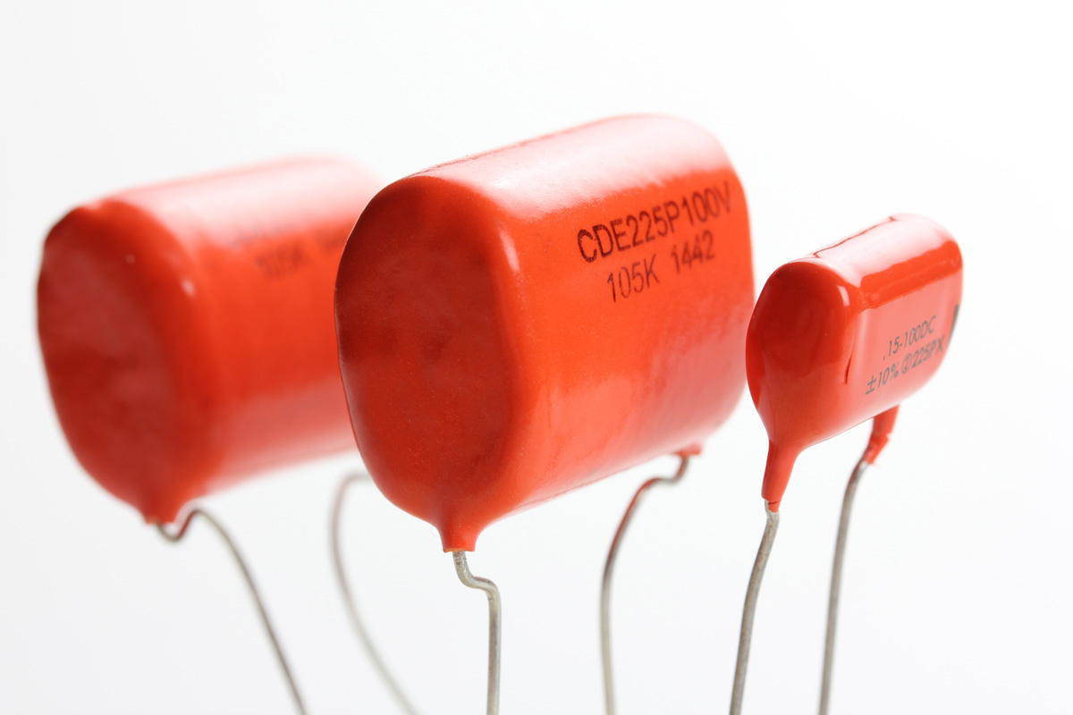
As explained above, the Orange Drop capacitor footprints have multiple pads for each lead. The pads on one side of the footprint are connected and the pads on the other side are also connected. This allows for installing capacitors with different lead spacing. If you're installing film caps in those positions (Rev D/F stock kit), simply place the capacitor where they fit making sure it's centered on the footprint. When installing Orange Drops, you'll want to use the two pads furthest apart. Those holes are slightly larger and appropriate for the thicker Orange Drops leads. Even though C7/C10 shows a + for polarity in the nested alternate capacitor, you can ignore it. The Orange Drops themselves are not polarized.

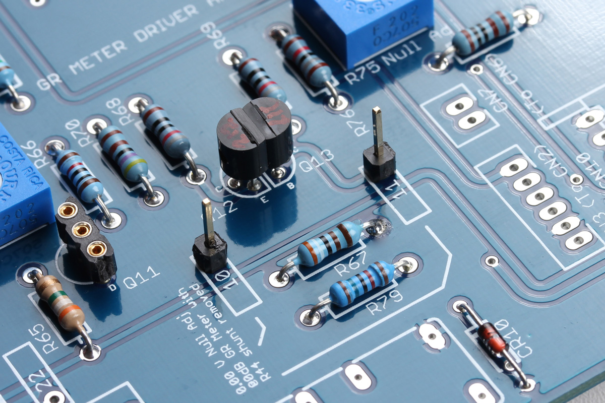
3 Pin Header and Shunt
Your compressor has a discrete meter section identical to the original units. During the calibration of the circuit you’ll need to take R44 out of circuit. This is done using a 3 pin header with a shunt. You can see the header inserted here next to R44 and it’s in the default R44 in-circuit position.
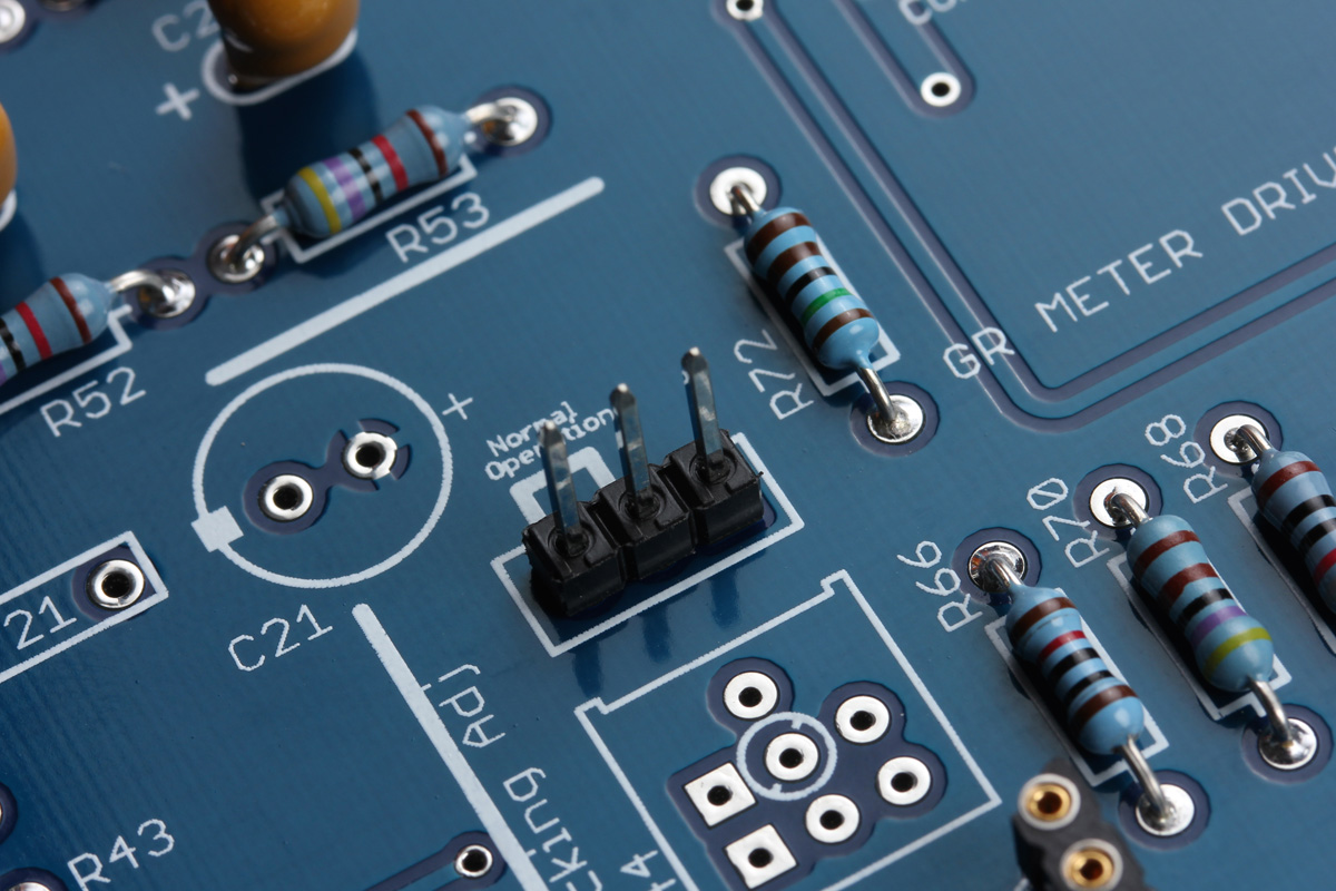
In normal operation (anytime other than completing this specific calibration step) you'll want R44 in circuit using the supplied shunt that will look like one of these cool guys.
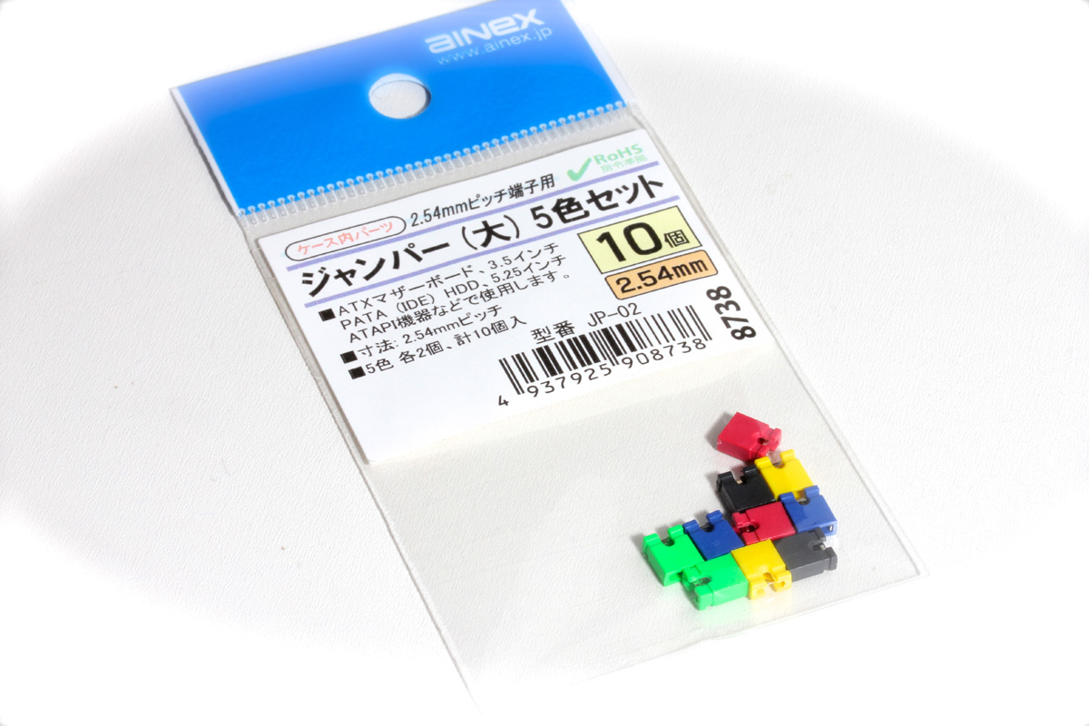
You'll only get one, it'll be black, and won't come in a cool bag but you can't have everything! In calibration, you'll start with it out of normal operation. You so can place it over the two pins on the right in the image above for now.
The FET/RACK build has several test points. Some are needed for calibration and others are provided for troubleshooting purposes. We do not include the test point hardware shown here in the kit. However, a cut lead from a diode or large capacitor will work just fine and you should have lots of those by now!
These are crucial as they allow you to test input and output levels while maintaining a load (XLR connection) on the circuit.
Installing many of these are optional, however, you should install pins or clipped leads in the test points labeled TP10 and TP11 on the Rev A/D. These will be used during calibration.
JST Headers
The JST headers are the white interconnects that receive either a wired housing or connect another small "daughter" PCB to the main PCB. They need to be installed using the correct orientation noted on the PCB silkscreen. It helps to install the wired connector while soldering the headers to the PCB.

This helps to stabilize and align the pins in the header. There is an opening on one side of the silkscreen that corresponds to an opening on the connector. CN3 and CN7 are shown installed correctly here.
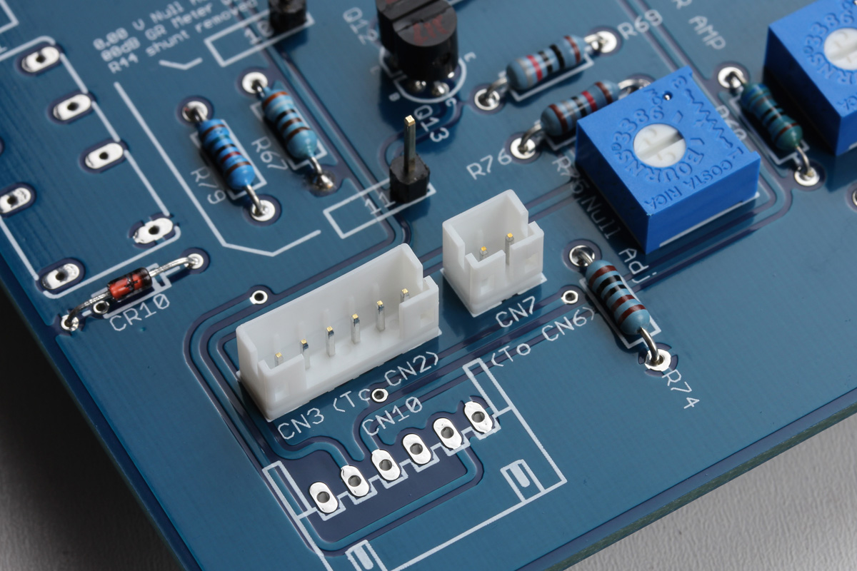
Followed by CN10. Note that on a batch of PCBs (late 2016/early 2017), CN10 had slightly too much plating in the holes making it hard/impossible to insert CN10 fully. If you have this issue, there is an easy fix. The outer pins (1 and 6) of CN10 have a little kink in them. Simply use a pair of needle-nose pliers to straighten out those two kinked leads, and CN10 will then press into place.
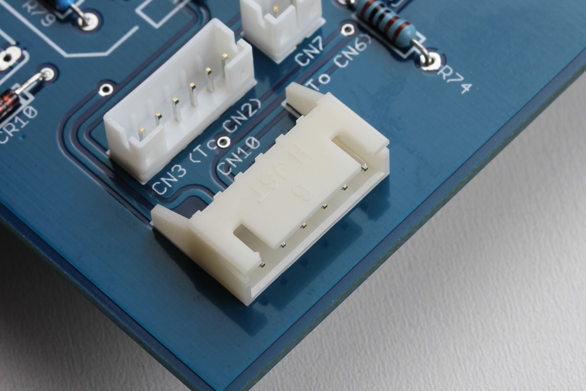
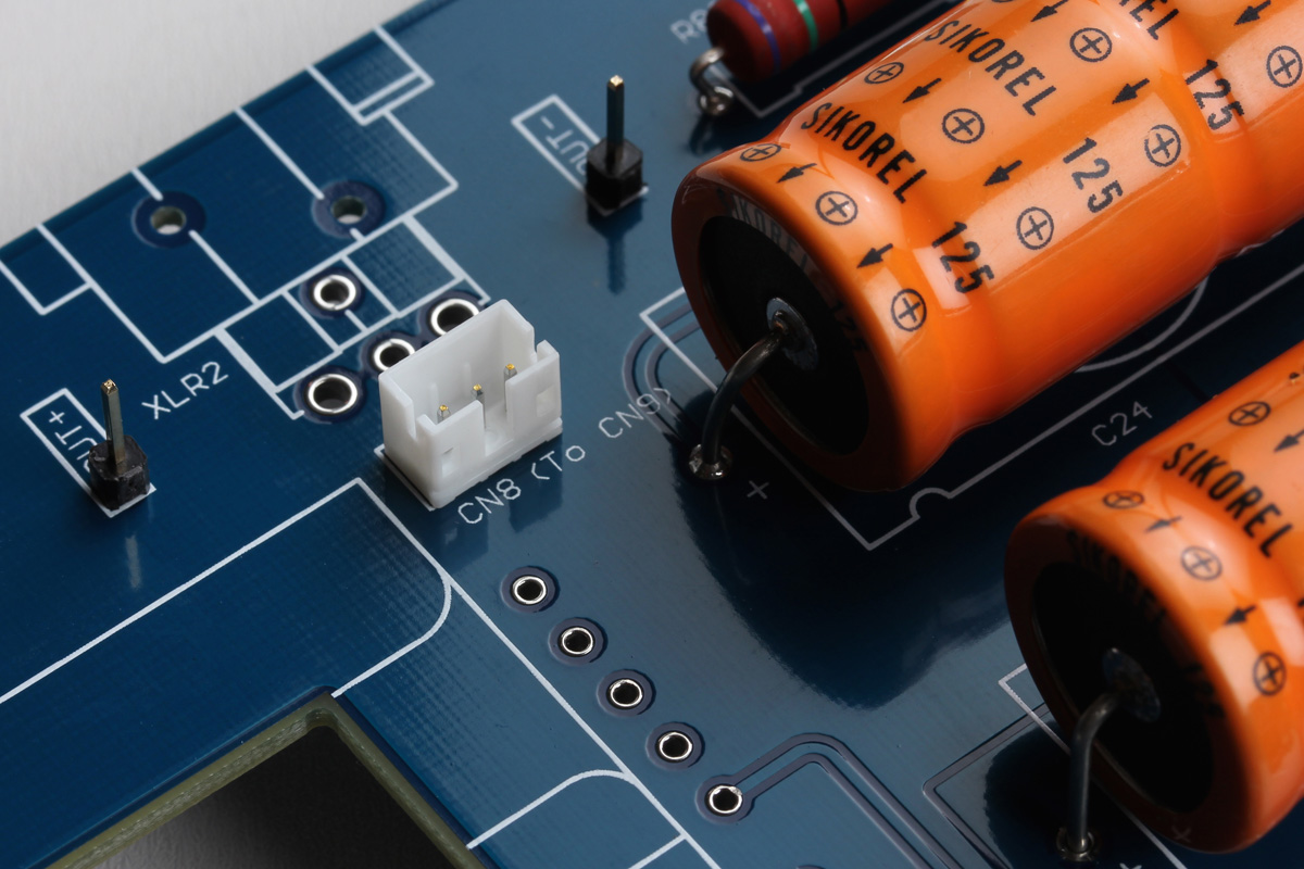
Then finally CN8 back by the output XLR.
CN17 is for the optional Active Link. That connector will come with the Active Link kit if you choose to install it.
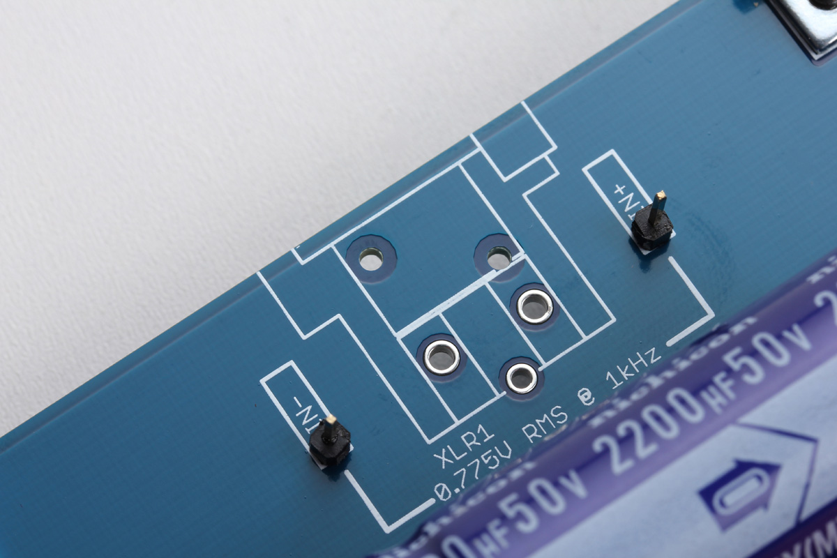
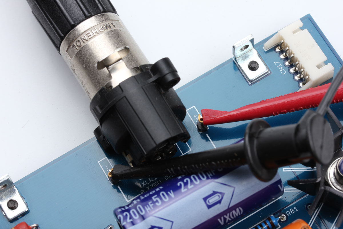
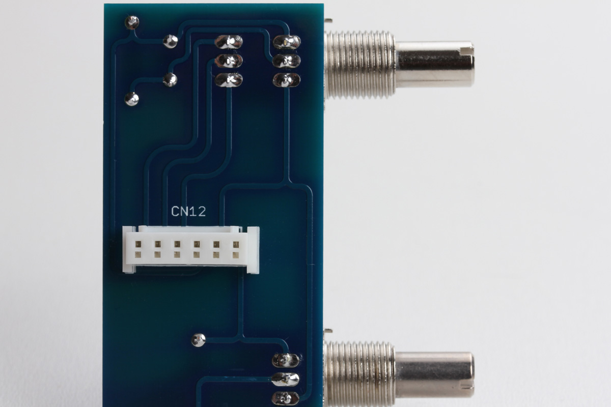
XLR and RCA Connectors
You have two XLR connectors to install on the rear of the PCB. The female connector is the input and the male connector is the output. The XLR connectors have plastic feet to help stabilize the part and they have corresponding holes in the PCB. These plastic leads should not be soldered! Only solder the tinned leads with pads.
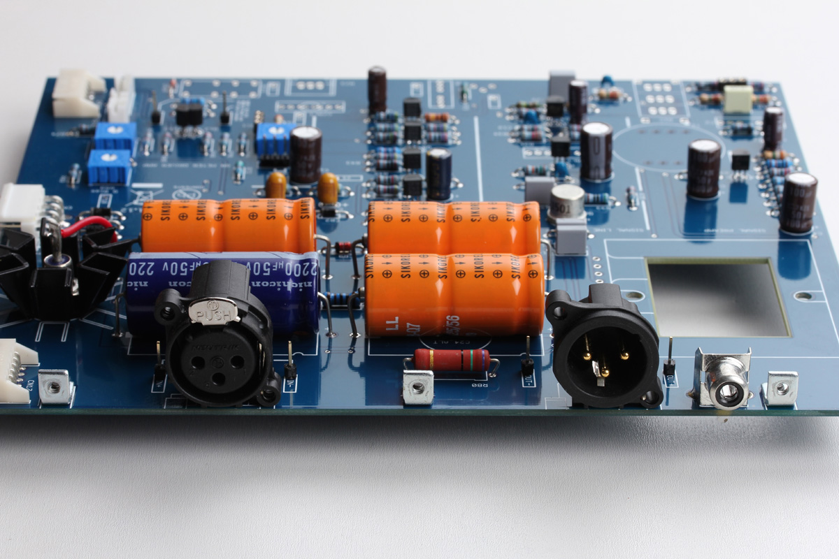
Below shows an image of the two XLR connectors and passive link RCA jack installed tight to the PCB.
Relay
Your FET/RACK has a relay switched active link option. Even if you never plan to use the active link, you need to install this relay switch. It's very straight forward and can only be inserted in the proper direction. PLEASE NOTE the relay has 8 total leads. It's very common for builders to see the 6 leads close together and miss the 2 leads off on their own. Make sure you solder all 8 leads!

Audio Transformers
Let's add some weight to this PCB!
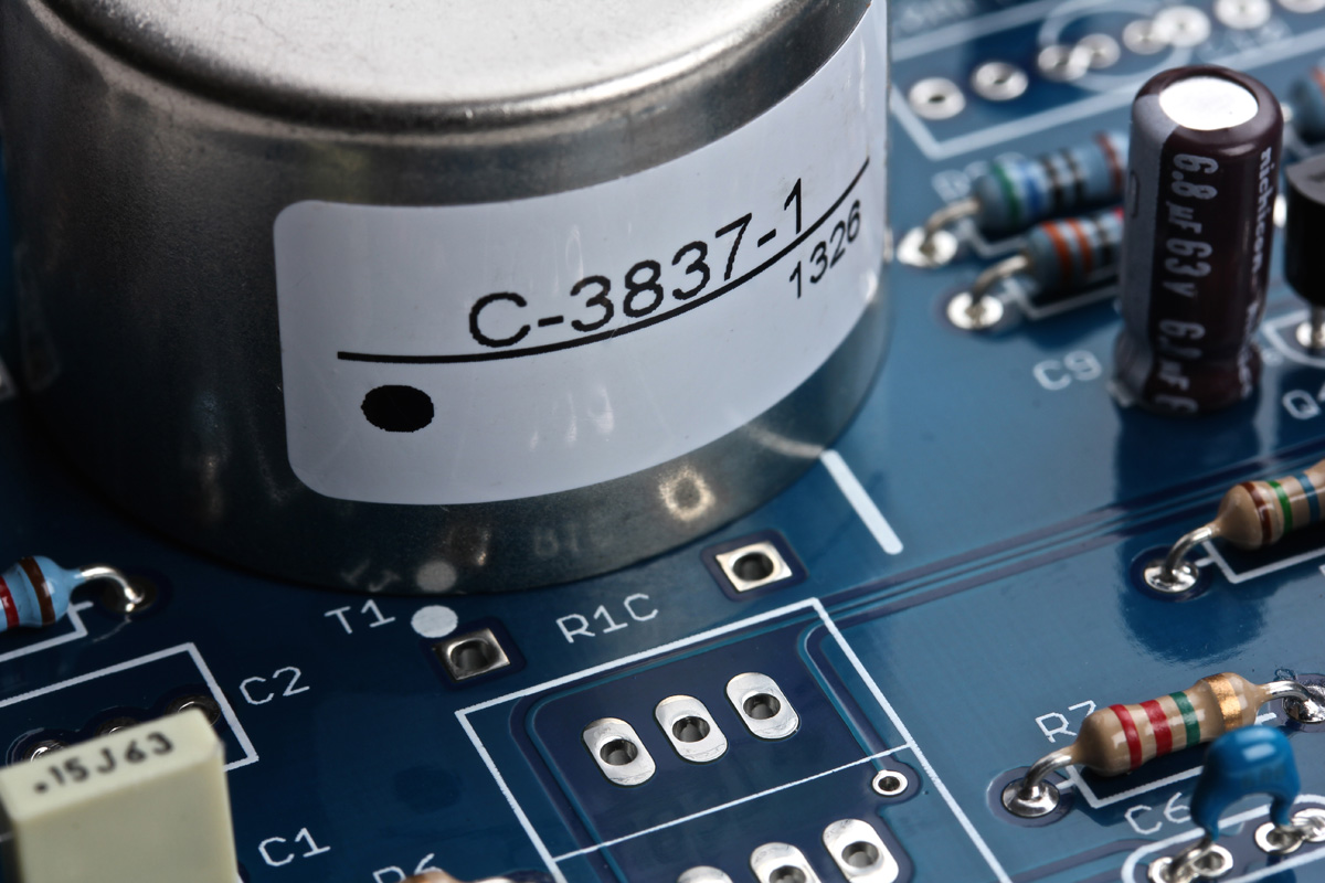
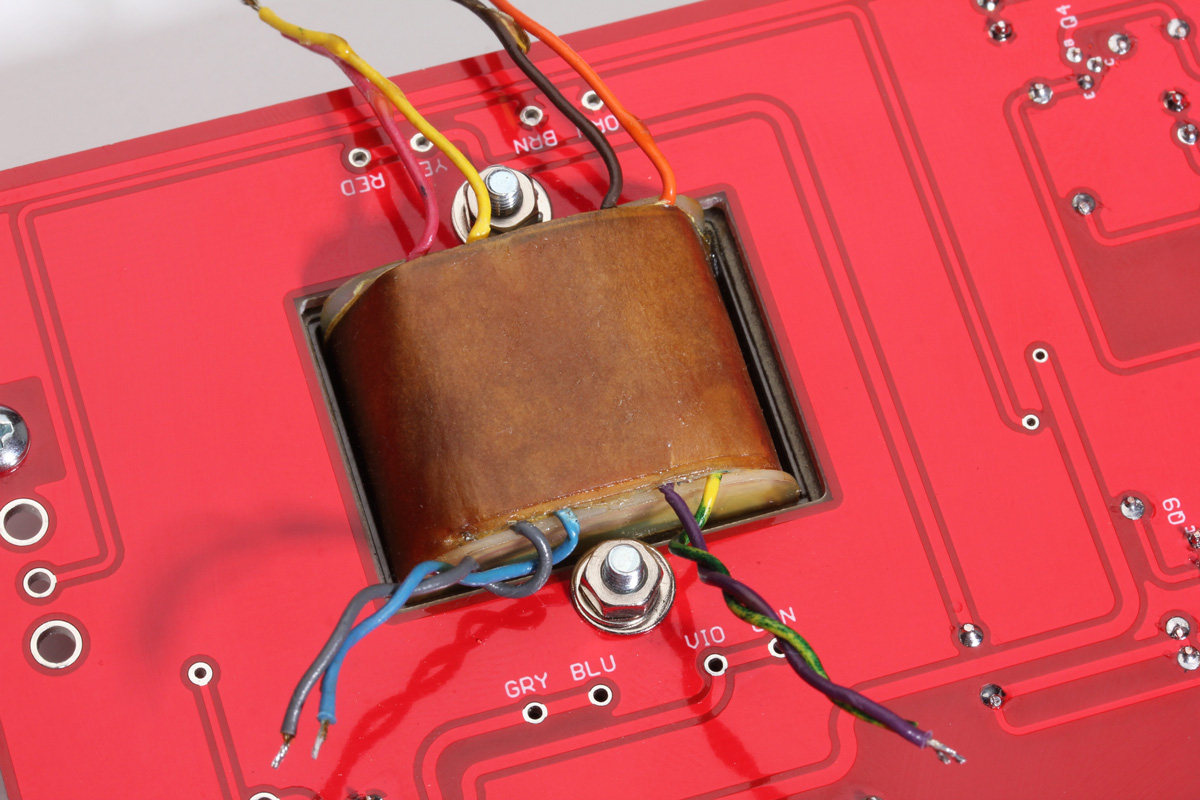
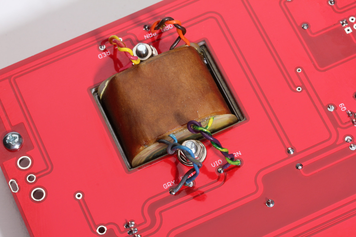
Start by mounting the input transformer. It must be installed in the proper orientation. Lead 1 is marked on the transformer with a small black dot as is the silkscreen on the PCB. Below you can see the proper orientation with the dots aligned. Solder all 6 leads of the input transformer. Be careful not to apply too much heat and solder.
The output transformer is mounted using the supplied hardware. There will be a bag containing two long #4 pan screws, nuts, and lock washers. The arrangement should be screw->transformer->PCB->lock washer->nut. In this top view, you can see the screw head and a flat washer which we do not include and is not needed. DO NOT overtighten the transformer. It is gapped and you can damage the transformer. Though that is highly unlikely.
Shown below is the 5002 output transformer used in the rev A and D. It may also be labeled "CM-96731" which is the Cinemag part number for the full-sized 5002.
![]()
On the bottom side, you can see the lock washer and nut along with the leads properly oriented towards the pads.
![]()
Once securely mounted you can begin soldering the leads to the bottom following the color-coding on the PCB. Trim the leads as you go to remove excess lead that could introduce noise into your output.
***Your output transformer may or may not have orange and yellow leads. The orange and yellow leads make the series connection on the secondary. If you have the wires, they are connected together on the PCB pads. If you don't have the wires, they are connected inside the transformer. If your transformer doesn't have orange and yellow wires, simply leave those pads empty.***
![]()
![]()
The rev F uses a B11148 output transformer. It is mounted the same and the leads can be twisted as pairs to reject noise and keep your build neat.
Front controls
Now we can mount the 3 deck t-pad input attenuator and single deck output pot. The t-pad in these images is blue, though your kit may include a blue or gray t-pad. They are electrically identical. The blue version does have an additional bracket surrounding the 3 pots. There are holes for the bracket legs on the PCB and they can be soldered to add stability. The output pot is the single deck grey pot marked "A250K" for the Rev A/D and "A100K" for the Rev F. The "A" indicates it has a logarithmic or audio taper and the 250K/100K indicates its total resistance. Make sure you have the right pot for your revision.
You can see the T-pad oriented below. Again, yours may be grey.

Once installed, trim the leads before soldering. Start by soldering one pin and confirm that pot is still set flush against the PCB, then complete the soldering of the other 8 pins and bracket legs if your T-pad is blue.

Nicely soldered.
You can install the output in the same manner. It only has 3 leads. When you're done, you should have something resembling the image below.
Now you should be finished with the main PCB. If you held off on installing the zero adjust trim pot, orange drops (Rev A only), or Q6 heatsink (Rev A/D only), you should install those now.
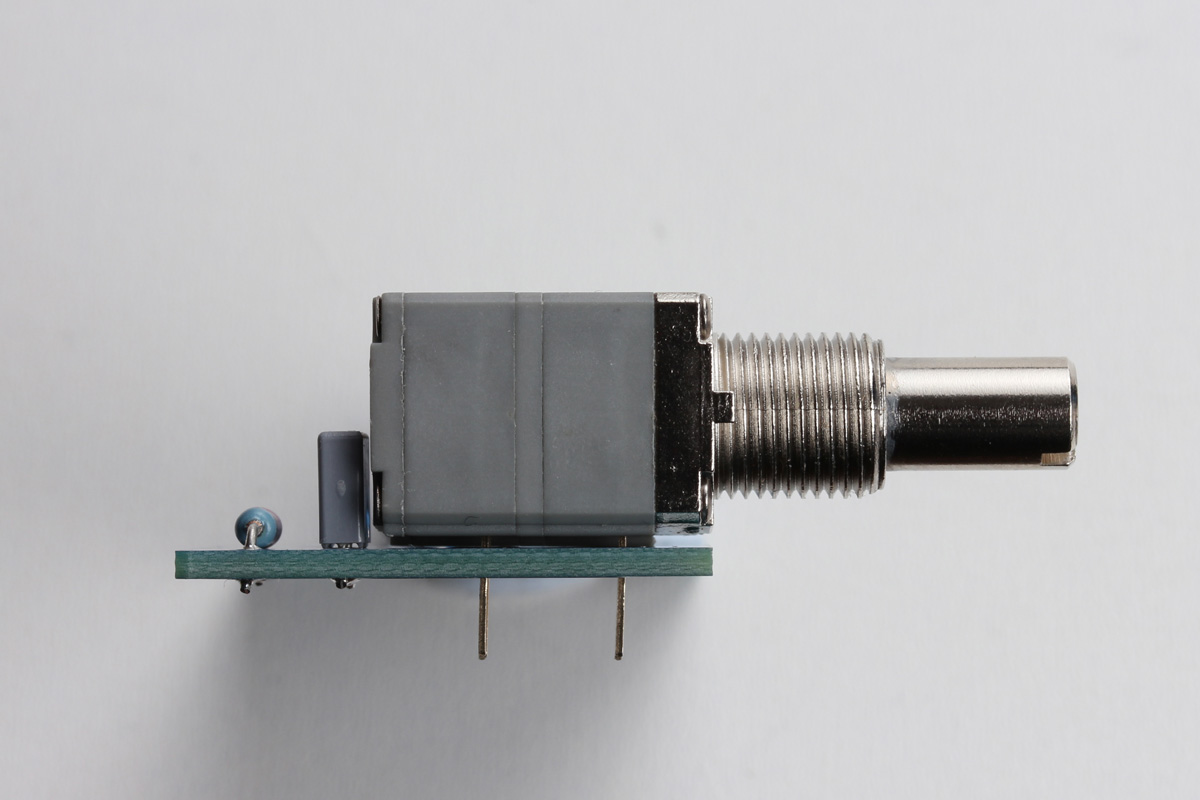
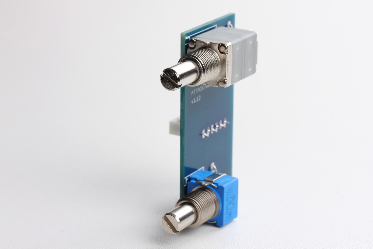
Attack and Release PCB
The attack and release network mounts to its own small PCB that connects to the main PCB using JST connectors. This board houses the two-deck grey attack pot (B25K) with switch and a blue (B5M) release pot. It also houses two resistors and a capacitor.
Start by mounting the resistors and capacitor. Next orient the attack pot as shown.
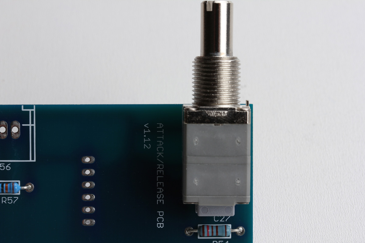
It is critical that the potentiometers and connector mount flush to the PCB.
Again, start by soldering one pin and confirm that the pot is still set flush against the PCB, then complete the soldering of the other 5 pins.

Repeat this process for the release pot and bottom-mounted connector. Take care when installing the release pot, the leads are easily damaged if they become unclipped from the tabs on the body. When you're done, your assembly should resemble the images below.
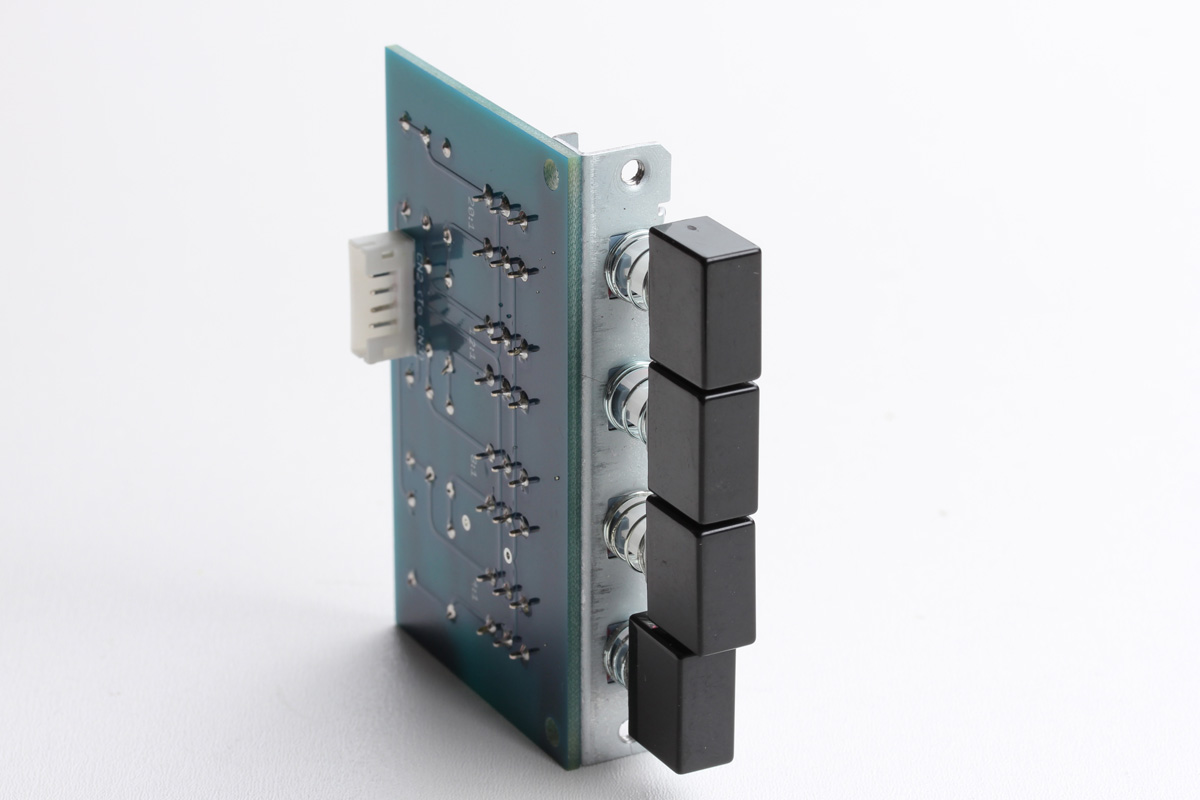
Ratio Switch
Assembling the ratio switch should be straightforward for you at this point. Use all the skills you've learned up until this point. Start with the resistors, mount the switch flush starting with on pin, and solder the rear-mounted connector flush.
You’ve made it! You’re now ready for the next step, final assembly your FET/RACK Compressor!